Design High Speed PCBs: Tips and Strategies
Design high-speed PCBs: impedance control, layer stacking, and crosstalk mitigation. Tools and strategies for 5G, USB 3.0, and HDMI layouts. Expert guide here!
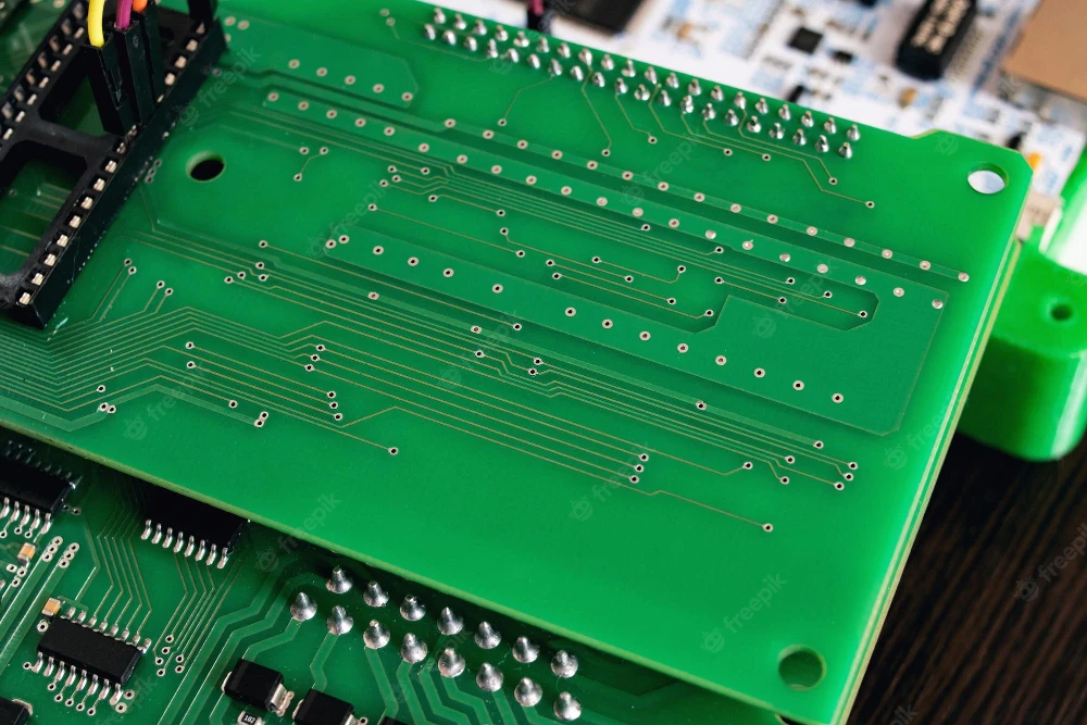
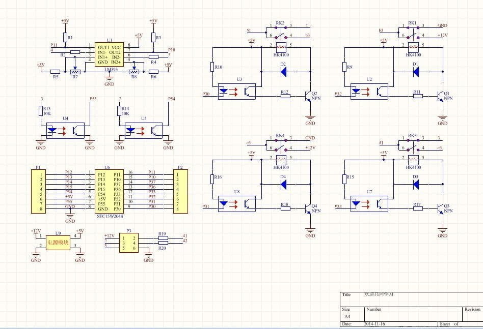
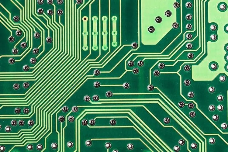
The pcb design is the process of creating a physical circuit board that can be used to power and control electronic devices. The process begins with a concept or idea, which is then converted into a schematic. Once the schematic is complete, the design is transferred to a physical board using a variety of methods, including etching, soldering, and milling. PCB design can be complex and requires a great deal of experience and knowledge to complete successfully.
Design high-speed PCBs: impedance control, layer stacking, and crosstalk mitigation. Tools and strategies for 5G, USB 3.0, and HDMI layouts. Expert guide here!
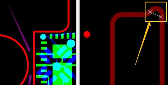
PCB Design Issues Drilling Hole Problem:Irregular hole ring design Risk:May confuse hole attributes Recommendation:Hole ring should be a hollow ring Problem:Holes without wire connections Risk:May lead to incorrect hole attributes Recommendation:Clearly define hole attributes in the source files Problem:Slot holes and circular holes overlap Risk:Unable to determine the required hole type Recommendation:If both need to
Looking for the best electronics pcb design software? Review 43 top free & paid suites with strong autorouter, dfa checks, reverse engineering & CAM tools.
43 Best Electronic Circuit & PCB Design Software Tools Read More »
PCB designers need to understand PCB trace basics to create high-performance printed circuit boards. From basic definitions to the types of traces, this article covers all the fundamentals you need. Working with printed circuit board (PCB) design software can be challenging at times. That’s because many technical terms and acronyms may seem confusing at first
This circuit is based on the PCB design of the capacitance test circuit of the PlCl6LF874 microcontroller. The specific contents are as follows. How the Capacitance Measurement Module WorksThe overall design principle block diagram of the capacitance measurement module is shown in Figure 1, including power management circuit, PICl6LF874 microcontroller, capacitive sensor, signal conditioning circuit,
PCB Design for Capacitance Test Based on Single Chip Microcomputer Read More »
What is DFM? Design for Manufacturing (DFM) is actually a bridge between R&D and production. It simplifies, optimizes, and improves product design to produce better products at a lower cost. Why is DFM So Important? The goal of the enterprise: low cost, high output, good supply capacity, and long-term reliable products. That is to say,
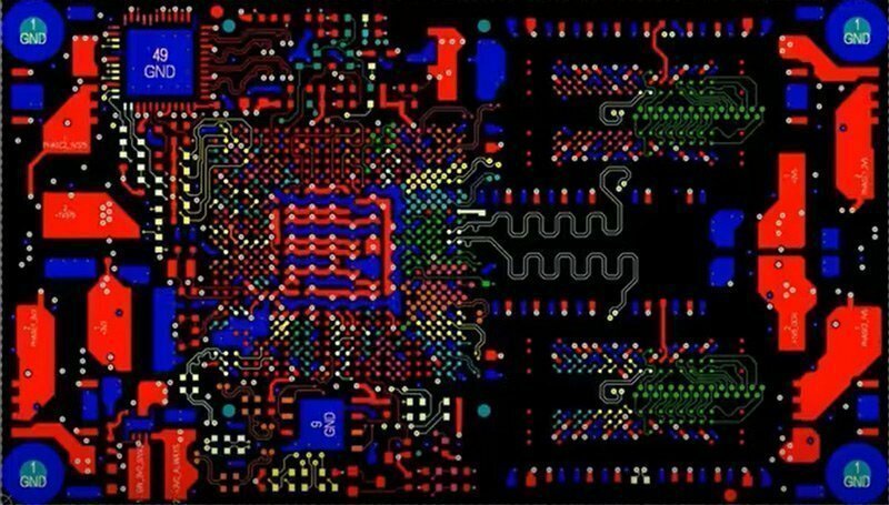
BGA is a commonly used component on PCB, usually CPU, NORTH BRIDGE, SOUTH BRIDGE, AGP CHIP, CARD BUS CHIP, etc. They are mostly packaged in bga type. In short, 80% of high-frequency signals and special signals will be pulled by this type of package. Therefore, how to deal with the routing of the BGA package
VR Gaming Technology Virtual Reality (VR) gaming technology is a rapidly advancing field that enables players to immerse themselves in a computer-generated 3D environment. With advances in hardware and software, players can interact with and explore a virtual world in a realistic way, making the gaming experience much more immersive. VR gaming technology is currently
Master PCB layout: trace width, ground planes, and component placement. Tips for signal integrity, thermal management, and manufacturability.
The car control panel is an essential part of any vehicle, allowing us to control its functions and make sure we have a safe and comfortable ride. However, over time, the car control panel can become outdated or malfunction, leading to a less enjoyable driving experience. Fortunately, reverse engineering can help us deconstruct the car
Deconstructing the Car Control Panel: Reverse Engineering for a Smoother Ride Read More »