
SEMICONDUCTOR FAILURE ANALYSIS
IC Failure Analysis Services
Identify electrical, thermal, package and process root causes with evidence-preserving diagnostics and an actionable engineering report.
Confidential review · Global project support · Test path selected from evidence
CONFIDENTIAL ENGINEERING REVIEW
Start Your IC Failure Review
Since 2008Engineering experience
Evidence-LedTest paths selected from symptoms
Multi-MethodElectrical, thermal and physical correlation
Confidential SupportNDA-friendly global projects
IC FAILURE SIGNATURES
IC failure signatures
we investigate
Semiconductor failure analysis begins with electrical behavior and operating history, then selects package-, die- and material-level methods that preserve the evidence needed to identify a defensible mechanism.
01
No output, leakage or parametric drift
Open internal paths, abnormal current, threshold shifts, degraded gain or other electrical behavior outside the device specification.
02
Intermittent or temperature-dependent behavior
Faults influenced by temperature, electrical load, timing, vibration or repeated cycling that require controlled reproduction.
03
EOS, ESD and localized overstress
Localized heating, current crowding, junction damage, oxide breakdown, electromigration or secondary electrical damage.
04
Package, bond-wire and die-attach defects
Delamination, voids, interface cracks, lifted bonds, die-attach anomalies and moisture-related package damage.
SEMICONDUCTOR ANALYSIS SEQUENCE
From electrical symptom to verified IC failure mechanism
The sequence protects package and die evidence while progressively moving from electrical characterization to a targeted physical finding.
01
Reproduce and characterize
Document the part, package, electrical symptom, operating conditions, reproduction rate and known-good behavior.
02
Screen the package
Use X-ray, C-SAM and external inspection to identify package, interface and interconnect evidence before opening the device.
03
Localize the active defect
Apply electrical characterization, thermal imaging or emission microscopy under controlled failure-reproduction conditions.
04
Verify physical evidence
Use decapsulation, targeted cross-section, FIB, SEM or EDS only after the likely failure site has been narrowed.
05
Correlate and report
Connect the electrical behavior, package or die evidence, process history and failure conditions to the most defensible mechanism.
ANALYTICAL CAPABILITIES
Core IC failure analysis methods
The test plan is chosen around the symptom, package, likely failure mechanism and evidence-preservation requirements—not from a fixed checklist.
01 / NON-DESTRUCTIVE
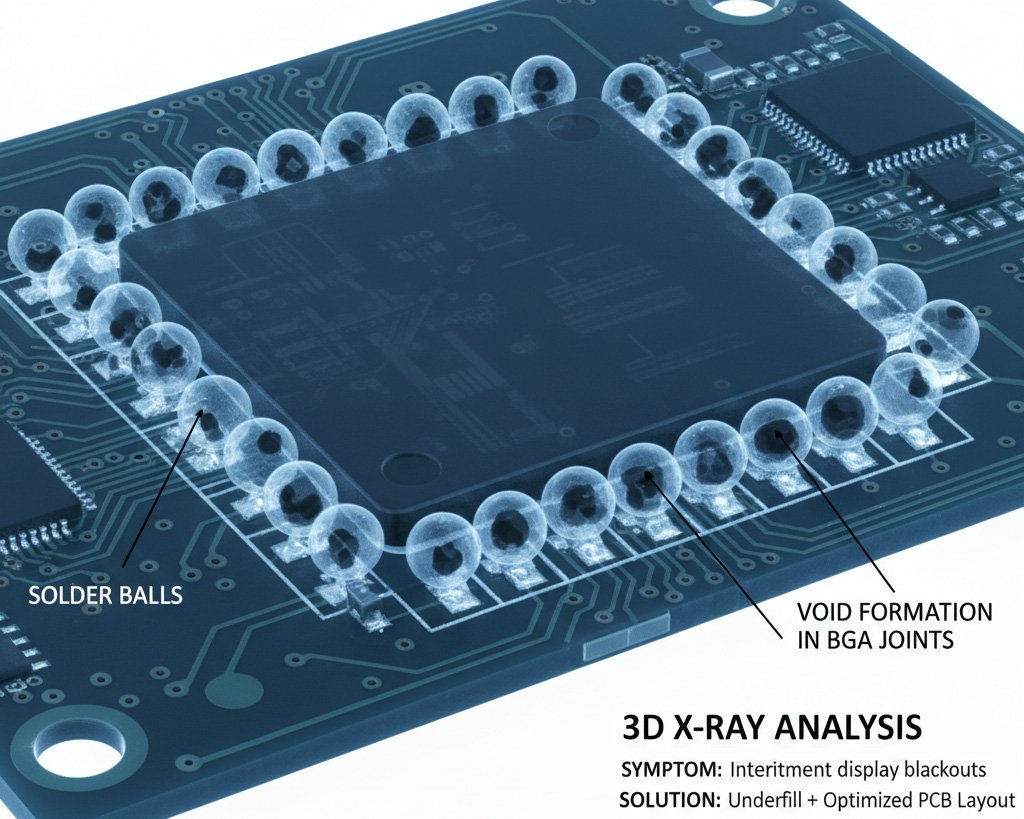
X-ray and acoustic microscopy
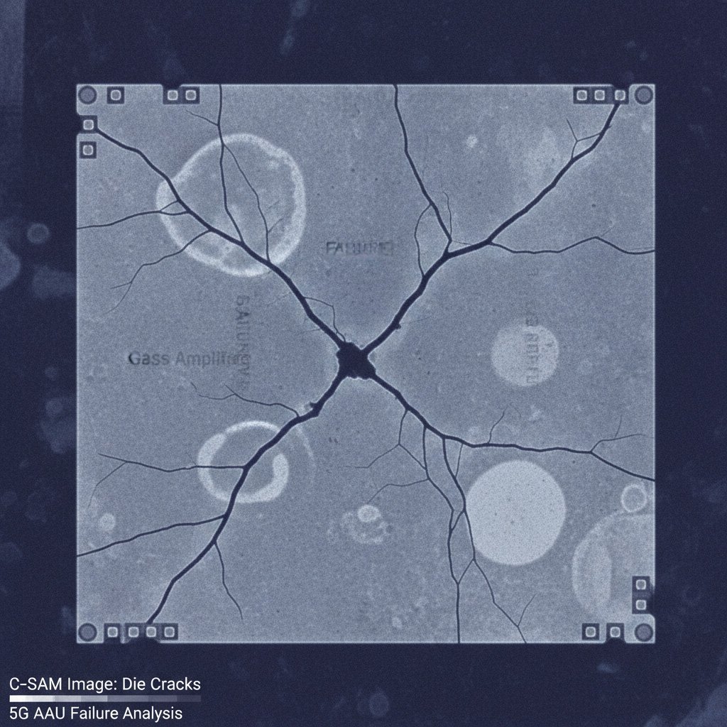
Inspect internal package structures, solder interfaces, voids, cracks, delamination and die-attach anomalies without opening the device.
- 2D and 3D package inspection
- Void, crack and interface comparison
- Evidence retained for targeted follow-up
02 / LOCALIZATION
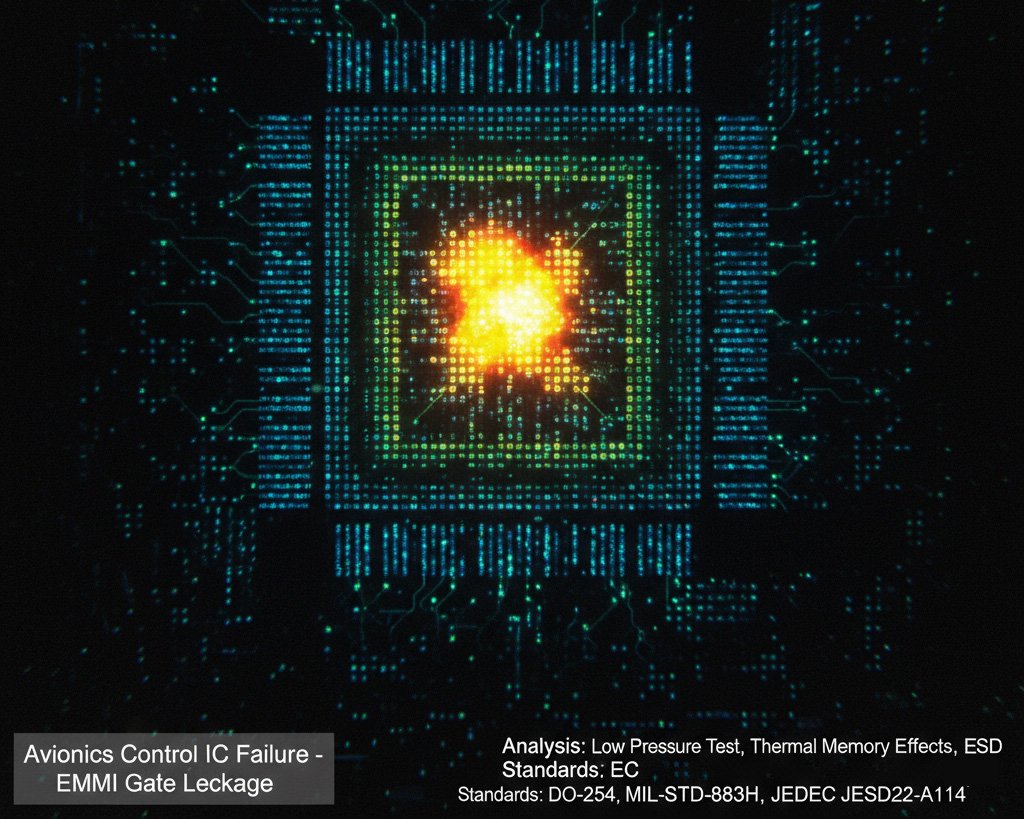
Thermal and emission localization
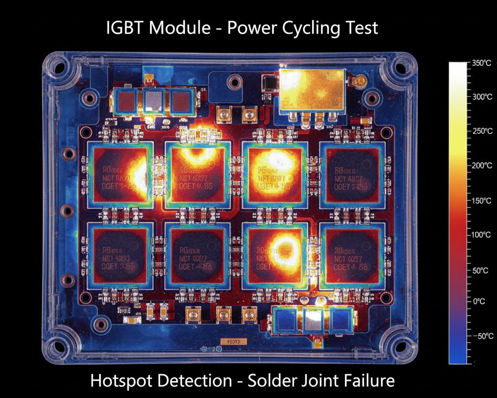
Locate abnormal heat or light emission while the device operates in a controlled failure-reproduction state.
- Compare suspect and known-good behavior
- Correlate temperature with load and time
- Prioritize evidence before physical analysis
03 / PHYSICAL EVIDENCE
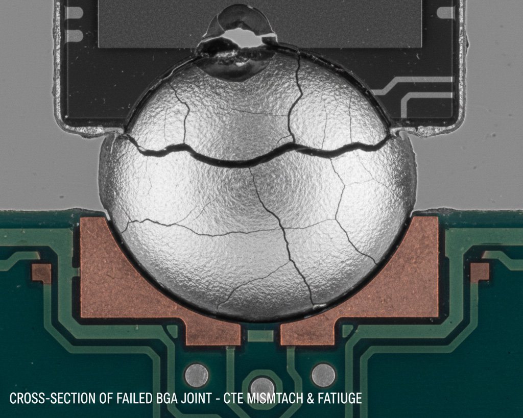
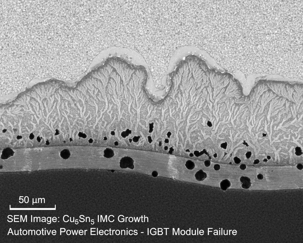
Cross-section, SEM and EDS
Expose selected structures and examine morphology, interfaces and elemental composition at the target location.
- Controlled sectioning and preparation
- High-magnification morphology review
- Elemental analysis and material correlation
METHOD SELECTION & EVIDENCE RISKS
Choose each IC analysis step for the failure mechanism
A useful test must discriminate between plausible mechanisms without destroying the evidence needed for the next decision.
No emission is not “no defect”
Open paths and some package faults may not emit detectable photons. Electrical behavior and complementary imaging determine the next method.
Localize before opening
Decapsulation and sectioning are most useful after X-ray, C-SAM, thermal or emission evidence has narrowed the target region.
Correlate, do not just image
A physical feature becomes root-cause evidence only when it explains the measured electrical symptom and the relevant operating history.
IC PACKAGE FAILURE PATH
Intermittent package failure under thermal cycling
Observed symptomA packaged device intermittently lost function after repeated temperature transitions.
Electrical localizationControlled tests narrowed the fault to a temperature-dependent internal connection.
Package evidenceNon-destructive imaging guided a cross-section that correlated an interface feature with the intermittent behavior.
Engineering actionReview the relevant package, interconnect, process and thermal-loading controls using the documented evidence.
IC ANALYSIS REPORT
IC failure analysis report deliverables
- Failure mechanism and confidence level
- Die, package and process correlation
- Annotated thermal, acoustic or microscopy evidence
- Electrical test conditions and reproduction notes
- Evidence limitations and recommended next steps
- Confidential engineering report
Helpful IC intake information
Device history and electrical context help protect the right evidence.
- Device or part number and package type
- Failure symptom and reproduction rate
- Operating voltage, load and temperature
- Manufacturing lot or field history, if known
- Known-good samples or comparison data
- Photos, logs, schematics or test files
BEFORE YOU SUBMIT
IC failure analysis FAQ
Still unsure which test method fits? Start with the symptom and available evidence; the analysis path can be defined during review.
What information should I send with the failed IC?
Send the part number, failure symptoms, operating conditions, reproduction rate, handling history and any available photos, logs, schematics or known-good comparison data.
Will the first tests damage the device?
The analysis normally begins with evidence review and non-destructive inspection. Any destructive step is selected only after its likely value, risk and evidence-preservation requirements are understood.
Can you investigate intermittent failures?
Yes. We can reproduce or bound faults using controlled temperature, load, timing and electrical conditions, then correlate the symptom with thermal, electrical or physical evidence.
What is included in the final report?
The report documents samples, test conditions, analysis sequence, annotated observations, findings, limitations and engineering recommendations appropriate to the available evidence.
START WITH THE FAILED DEVICE AND ELECTRICAL SYMPTOM
Need an engineer to review your failed IC?
Share the part number, package, electrical behavior, operating conditions and any available evidence. We will recommend the next IC analysis step.