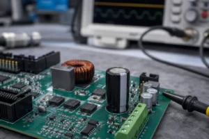
How to Choose an Electrolytic Capacitor for a PCB Power Stage
Learn how to choose an electrolytic capacitor for PCB power stages by checking ripple current, ESR, temperature, package layout, and the failure modes that cause repeat board repairs.
Schematic & Gerber restoration
MCU/CPLD code restore access & backup
1:1 exact hardware replication
BLE & Classic BT wireless solutions
Precision PID & thermal management
High-efficiency motor drive control
Industrial RS485/RTU communication
Custom STM32/ESP32 firmware & HW
Calculate the PCB trace width based on temperature rise, current, and copper thickness (IPC-2152).
PCB prototyping is a way to make your product without the need for expensive manufacturing processes. This will give you plenty of opportunities to test different features before mass production begins which could result in lower costs down the road.
PCB prototyping service is the first step to manufacturing PCBs. It helps to speed up the design process for any product or device before it is mass-produced and/or sold on the market, in order to ensure that all engineering specifications are met. This can save time, money, and frustration when it comes down to ordering boards without having any idea of what they’ll look like or how much it’ll cost you until after a few rounds of revisions are made.

The design process begins with a PCB layout. From there, we will specify what components are going to be used on the circuit board and how we placed them on the individual layers of it.

This allows customers who wish to prototype their designs or test new technologies saving time and cost associated with prototypes that have been tested fully at various stages along the way.

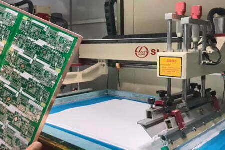
PCB prototypes are manufactured by printing the circuits on a rigid substrate such as FR-4. In order to print circuitry, it is necessary first to model or scan an object with your CAD software and then extract the individual layers.

Cutting through conductive tracks in desired locations using drills or lasers, etching away unwanted material if needed (usually a chemical agent), and finally attaching additional materials like solder masking tape , silk screening.
PCB prototyping boards are different types of PCBs designed for testing and evaluation. These prototypes can be used to evaluate the performance of your design prior to starting mass production or assembly. PCB Prototype Boards include:
Below are our specific pcb design process and prototype production:
The first step in PCB prototyping is to develop a design for the PCB. It is necessary to determine all the components that will be needed, the interfaces between the components, and the physical features of the PCB. After the design is complete, it can be sent to a PCB manufacturer (or ‘fabricator’), who will produce a proof-of-concept board based on your design.
There are several different ways that you can create a design for a PCB:
1) You can hand-draw your design using the tools in your drawing program of choice (e.g., Adobe Illustrator).
2) You can use circuit creation software (such as KiCad) to automatically generate your design from scratch.
3) You can copy/paste parts from online libraries into your own drawing file or circuit creation software (this is often called ‘schematics plagiarism’).
4) You can start with an existing open-source or commercial library that has been created by someone else (there are many such libraries available).
A product’s manufacturing process and component locations are determined by the schematic. It includes information about materials, hardware, and components, as well as information about how the product is manufactured. There are several steps in creating the schematic from a pcb.
You must also create a bill of materials (BOM). This inventory includes all the components and materials required for production as well as how much of each is necessary. Manufacturers will use this document to ensure they receive the correct parts when sourcing your materials. Each part is listed with the following information: quantity, reference designators, value, quantity, footprint, and manufacturer part number.
After you’ve determined where everything should go, you must decide how to connect them using traces. Routing is important to consider because it affects power levels, signal noise generation, and signal noise sensitivity. When you’re using a PCB design software, the netlist you’ve already created is used to create routing. These programs can often determine the optimal route based on the number of available layers and other factors. This can take a long time, particularly for large circuit boards or those with many components.
Before the fabrication process begins, it’s important to verify that your design is properly implemented. Inferior thermal channels, inconsistent copper thicknesses, large PCB sizes, and numerous PCB layers may cause hot spots and inconsistent temperatures. Make sure that the PCB maintains a constant temperature throughout the manufacturing process. A thermal test, as well as a design-versus-schematic (LVS) test, an electrical rule check (ERC), and an antenna test are all required. The manufacturer may perform other quality control checks as well.
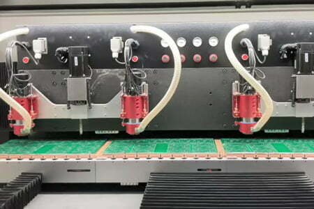
In the Fabrication phase, PCB Prototype fabrication company will create a proof-of-concept board for you. There are many steps involved, including: developing a photograph film, printing inner layers, copper plating, drilling holes, solder paste stenciling, pick and place, assembly, and more.
The ultimate step in PCB prototype assembly is a comprehensive test of how well it performs under the conditions it will be utilised in. If testing reveals problems with your design, you may need to alter your prototype and test it again to ensure that it works properly. If you’re pleased with your prototype’s performance and quality, you can go further for a full production of the board.
pcb prototyping costs can vary depending on factors such as the size of the project, complexity of electronic circuits, or required materials that are used with pcb prototypes. The total cost of prototyping pcbs usually includes the cost of the printed circuit board material, pcb production, component cost, and pcb testing.
What you will pay for a prototype of a printed circuit board PCB depends on many variables. Most PCBs need to be made of four layers, of course adding more layers can help reduce board size, but it will increase the cost of the board.
The production process mainly includes PCB layout, core board production, inner-layer PCB layout transfer, core board drilling and inspection, lamination, drilling, copper chemical precipitation on hole walls, and outer-layer PCB layout. Transfer, outer PCB etching, etc.
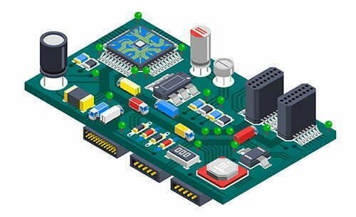
It's one of the SMT (Surface Mount Technology) components, consists of the actual all surface-mount devices, and manual soldering. Compared to production and assembly of circuit boards, components cost less.
Electronic components must be tested before they are soldered to the PCB circuit board, the testing cost vary depending on the test methods. It consist of manual visual inspection and automated machine inspection.
Quality Control of Prototyping PCB is a complicated process that requires the right personnel and equipment. Our factory have control engineers to ensure quality standards throughout an entire production line. Quality control involves checking each individual step in production, from sampling raw materials to inspecting finished products for defects. The following are some ways we implement quality control:


Submit your requirement details of pcb assembly on the form, upload your files is available. And we'll reply to you within 24 hours.

Our expert will contact you for the project details, reply to you with a quotation, and confirm the order after recieving your payment.

The sample will be arranged to produce as you expect within 1 day, then we confirm with you the appearance and function.

Lead time: At last, your sample w'll be finally shipped to you within 7-15 days. It'll depends the shipping way you choose.
We have been specializing in PCB prototyping and PCBA manufacturing services for over 15 years, serving more than 3,000 customers worldwide.
We possess the latest professional production equipment to handle the PCB and PCBA manufacturing process and provide complete service from PCBA design analysis, program design, sample, and mass production as a one-stop solution.
Equipped with a professional PCB board production line, SMT processing production line, industry-leading production equipment and professional technical management team.

Learn how to choose an electrolytic capacitor for PCB power stages by checking ripple current, ESR, temperature, package layout, and the failure modes that cause repeat board repairs.

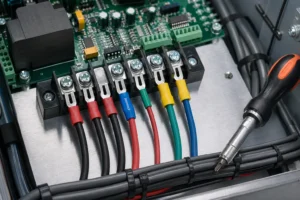
A spade connector is useful when electronics wiring needs quick service access, but it becomes a liability if vibration, poor crimp control, or hidden screw joints can let the fork walk loose.
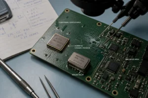
Hermetically sealed components earn their cost only when moisture, outgassing, pressure cycling, or long service intervals make ordinary coating and enclosure strategies unreliable.
PCB prototyping services turn a controlled design package into a small build used to expose layout, fabrication, assembly, component, and functional risks before volume production. A useful prototype is not merely a quick bare board: its stackup, materials, copper, parts, assembly process, and test conditions should represent the questions the build must answer. Clear revision control and acceptance criteria prevent a successful prototype from becoming an undocumented one-off.