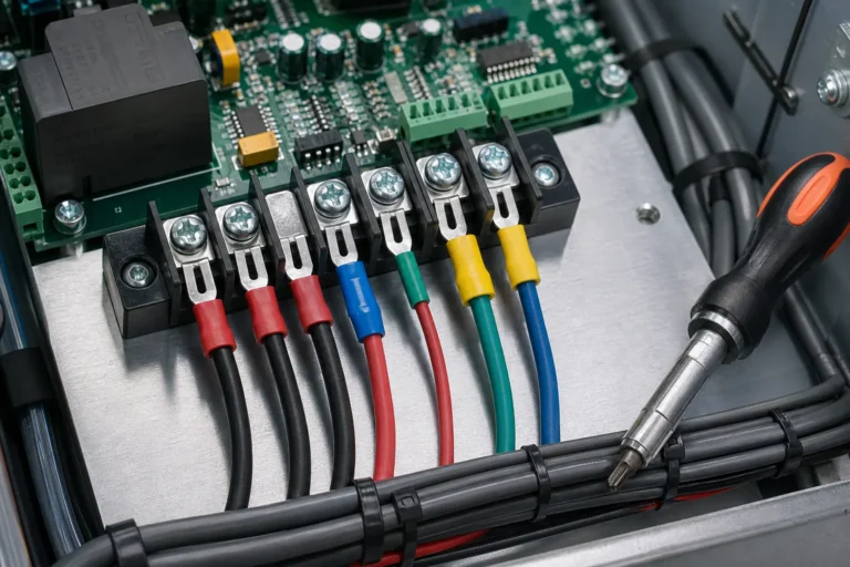
When a Spade Connector Makes Sense in Electronics Wiring
A spade connector is useful when electronics wiring needs quick service access, but it becomes a liability if vibration, poor crimp control, or hidden screw joints can let the fork walk loose.

A spade connector is useful when electronics wiring needs quick service access, but it becomes a liability if vibration, poor crimp control, or hidden screw joints can let the fork walk loose.
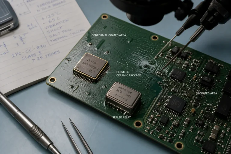
Hermetically sealed components earn their cost only when moisture, outgassing, pressure cycling, or long service intervals make ordinary coating and enclosure strategies unreliable.
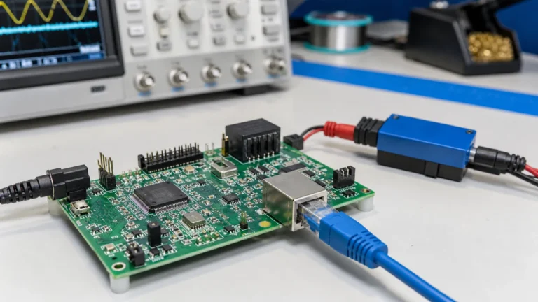
Energy Efficient Ethernet only earns its keep when the PHY, link partner, measurement setup, and board-level signal path all support low-power idle cleanly.
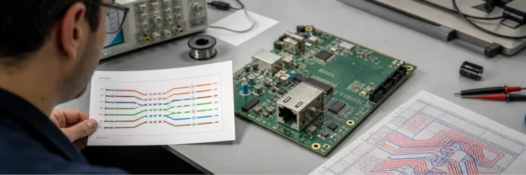
RJ45 pinout work gets risky when connector viewpoint, differential pairs, magnetics, and PoE details stop matching each other on the PCB.
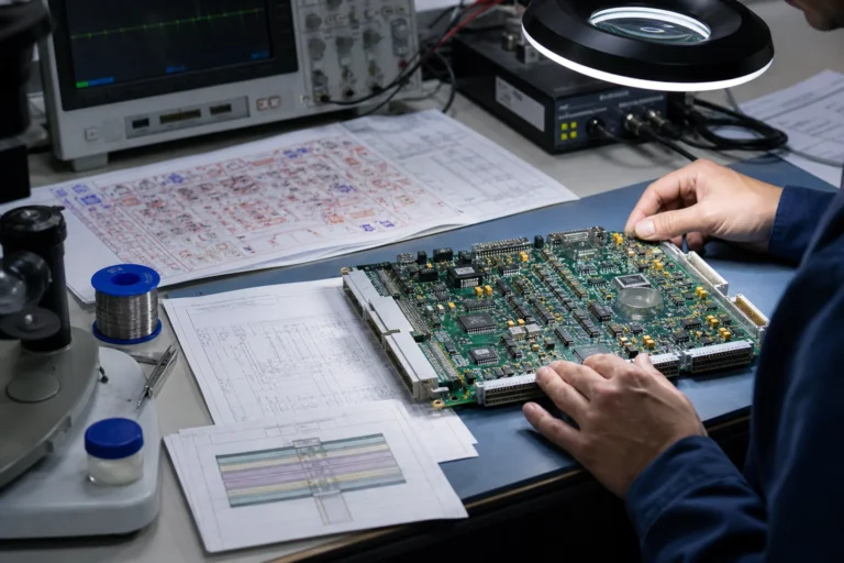
NASA PCB design guidelines are most useful when they turn layout, assembly, and verification into one reliability workflow instead of a copied list of conservative-looking rules.
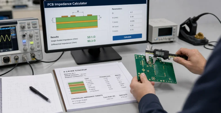
A PCB impedance calculator only helps when the stackup, copper, solder mask, and release assumptions still match the board that fabrication and assembly will actually build.
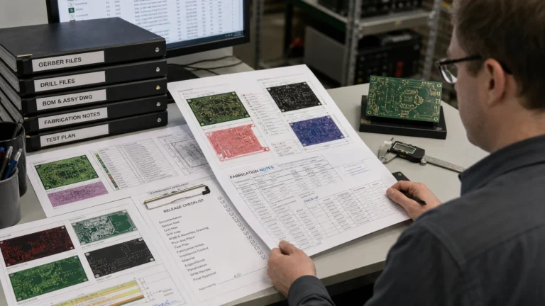
Gerber files only speed PCB fabrication when drill data, stackup notes, version control, and manufacturing intent are released as one coherent package.
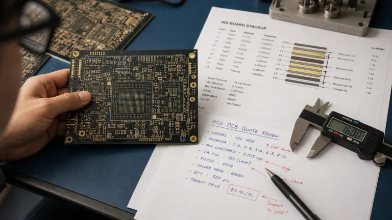
HDI PCB cost is driven by microvia structure, lamination count, imaging limits, inspection burden, and assembly risk long before a supplier sends the final quote.
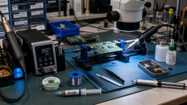
A useful soldering kit for PCB rework is built around thermal control, board handling, inspection, and cleanup, not just an iron and a spool of solder.
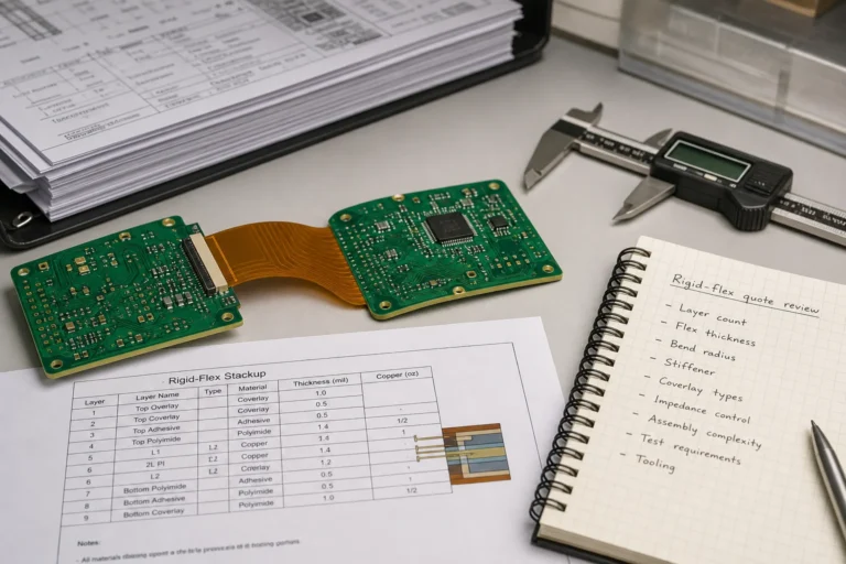
Rigid-flex PCB cost is driven by bend-zone rules, materials, lamination cycles, stiffeners, yield risk, and quote details that ordinary multilayer pricing does not capture.