When it comes to designing high-speed PCBs (Printed Circuit Boards), there are a few tips and strategies that must be taken into account to maximize performance. High speed PCB design is a complex process that requires a lot of attention to detail to ensure that the boards operate as expected. In this blog article, we will discuss the various aspects of high-speed PCB design, from understanding the guidelines to selecting the right material to strategies for optimizing performance. We will also look at the benefits and challenges associated with high speed PCB design and provide practical steps for designing high-speed PCBs. Finally, we will talk about testing and verifying the performance of high-speed PCBs and troubleshooting design issues.
What Is High Speed PCB?
High Speed PCBs (Printed Circuit Boards) are special circuits designed to operate at higher frequencies and high data rates than standard PCBs. In generally, A high-speed PCB comes with these characteristics:
- The signal speed is larger than 50MHz;
- The signal rising or falling edge is less than 50 ps;
- The transmission path length of the signal is longer than 1/6 λ;
- Severe skin effect and ionization loss occur when the signal is transmitted.

They are built using higher-grade components and specialized materials to reduce electrical noise and interference, and to improve signal integrity. High Speed PCBs are used in applications such as high-speed digital communications, high-speed data processing.
Introduction to High Speed PCB Design
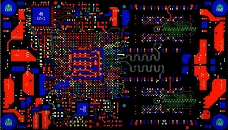
High speed PCB design is a specialized process used to create boards that are capable of handling high speed signals. It involves designing the PCB with a specific focus on the signal integrity and the electrical performance of the board. This means that the components on the board must be carefully selected and placed in order to ensure that the signals propagate properly and the board is able to withstand the high speeds.
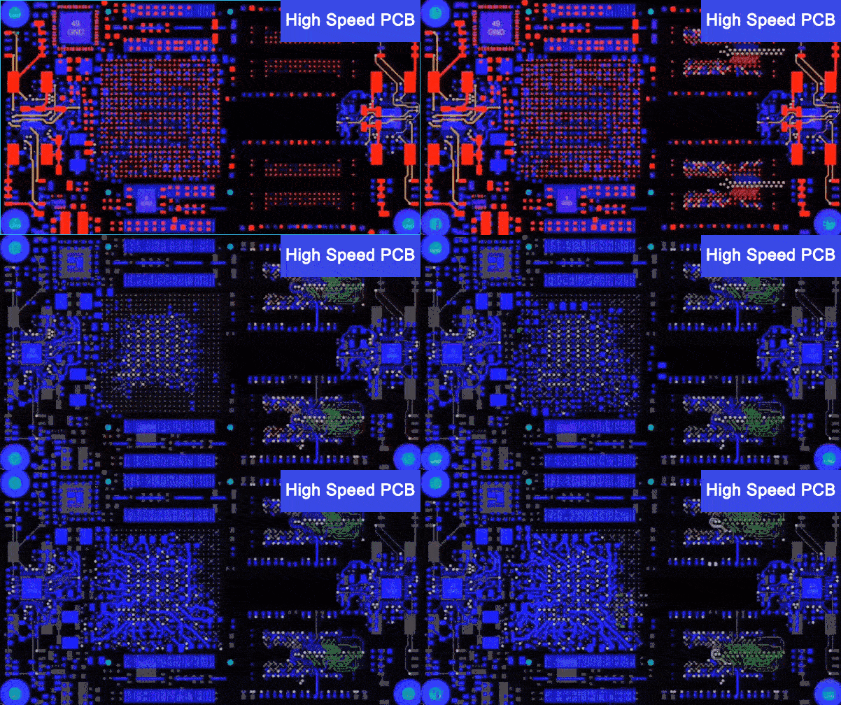
High speed PCB design also involves taking into account the physical limitations of the board, such as the trace width and spacing, as well as the interference between components. In order to ensure that the board is able to handle the high speeds, the components must be placed and routed properly and the board must be designed with the proper materials.
High Speed PCB Design Guidelines
When designing a high-speed PCB, it is important to understand the guidelines that must be followed to ensure that the board can handle the high speeds.
Impedance control
Impedance control is an important requirement for high speed PCBs as it helps ensure the integrity of the signals being transmitted. The most common requirement is to maintain a characteristic impedance of 50 ohms or 100 ohms over the length of the trace.
Use controlled dielectric materials
The most common method used to control impedance in a PCB is through the use of controlled dielectric materials (e.g. FR-4). These materials have a specific dielectric constant that can be adjusted to create a specific impedance for the desired signal path. In addition to the FR4 materials, other materials can be used in high speed PCB design, such as polyimide, ceramic, and glass-filled epoxy. Each of these materials has its own unique characteristics that must be taken into account to ensure that the board can handle the high speeds.
Length matching traces
Length matching traces is a technique used in circuit board design to reduce the electrical noise. It involves making sure the length of traces between two different components is equal so that the signals arrive at the same time. This prevents noise from one trace interfering with the signal on another trace.
Reduce vias
Other factors that must be taken into consideration when controlling impedance on a high-speed PCB include the presence of vias, which can cause reflections and reduce the effectiveness of the impedance control. Additionally, if multiple layers are used, the impedance between the layers can be affected by the presence of copper planes, which must be accurately placed and sized to minimize any impacts to the signal integrity.
Impedance test equipment
In order to accurately measure the impedance of a PCB, specialized test equipment must be used. This test equipment is typically used to measure the differential impedance of the trace as well as the return loss of the signal. By using these tests, engineers can accurately determine the impedance of their PCBs and make any necessary adjustments to ensure that the desired impedance is achieved.
Trace width and spacing
The trace width and spacing of high speed PCBs are important design considerations that must be taken into account in order to ensure reliable signal integrity. Trace width is the width of the conductive line on the board, while spacing is the gap between two traces. Both of these characteristics are critical factors when designing a high-speed PCB as they directly affect the electrical performance of the board.
Trace width
Trace width should be chosen such that the resistance of the trace is low enough to avoid signal attenuation. Depending on the application, trace width can range from 0.25mm to 0.8mm, with thinner traces being used for higher speeds. The optimal width of the trace should be chosen based on the current carrying capacity of the trace, the frequency of the signal, and the layer stackup of the board.
Spacing
Spacing between traces is also an important consideration for high speed boards. Spacing should be selected to minimize crosstalk between signals and ensure adequate isolation. Generally, trace spacing should be no less than 1.5 times the trace width. This will provide adequate isolation between the two signals without creating too much parasitic capacitance.
EMI shielding
Electromagnetic interference (EMI) shielding is a critical requirement for high speed printed circuit boards (PCBs). EMI shielding helps prevent unwanted interference from other electronic components or external sources such as radio waves from entering the PCB or components, which can cause performance issues or even complete system failure. To ensure proper EMI shielding, designers should incorporate the following measures into their high speed PCB design:
Utilize appropriate materials and components
To ensure effective EMI shielding, materials used in the board design should have a high electrical conductivity and be as thick as possible to minimize signal penetration. Common materials used for EMI shielding include copper plates, aluminum foil, and polyester tape.
Incorporate EMI gaskets
EMI gaskets are designed to provide a tight barrier between the PCB and other electronic devices. They typically consist of a conductive material such as copper or aluminum foil surrounded by a flexible rubber or plastic material.
Place ground planes strategically
Ground planes are used to help reduce signal noise. By placing ground planes near sensitive components, designers can limit the amount of noise that reaches them. Additionally, grounding planes also help reduce signal reflections.
Utilize EMI filters
EMI filters are used to block unwanted signals from entering the PCB. These filters can be placed in line with power and ground lines or at the input and output lines of signal sensitive components.
By incorporating these EMI shielding measures into their high speed PCB design, designers can ensure reliable operation and consistent performance.
Power and ground planes
The power and ground planes must be carefully designed and routed to ensure that the board can handle the high speeds. Power isolation and ground splitting are often required between different circuits to reduce signal interference. Such as analog circuit and digital circuit, weak signal circuit and strong signal circuit, etc.
basic requirements:
- The power layers or ground layers in different areas should be connected together at the power inlet, usually in a tree structure or finger structure;
- The ground wire division method of different functional circuits, the division gap and the edge of the board shall not be less than 2 mm;
- Different types of power supply areas and ground areas cannot cross each other.
The Benefits of Utilizing High Speed PCB Design
Several benefits come with utilizing high speed PCB design.
One of the most important benefits is that it allows for faster signal propagation, which means that the board can handle the high speeds required for high-performance applications.
Additionally, high speed PCB design allows for smaller components and traces, which means that the board can be designed with less space and can be more compact.
The other major benefit of high speed PCB design is that it allows for better noise immunity and signal integrity. This means that the board can handle the high speeds without losing any of the data or signals that are being transmitted. Finally, high speed PCB design allows for better power efficiency, which means that the board will be able to handle high speeds without consuming too much power.
Challenges of High Speed PCB Design
There are also a few challenges that must be taken into account.
One of the biggest challenges is that high speed PCB design is a complex process that requires a lot of attention to detail to ensure that the board can handle the high speeds.
Additionally, high speed PCB design requires the use of specialized materials and components, which can be expensive and difficult to source.
Finally, high speed PCB design is a time-consuming process, as it requires a lot of testing and verification to ensure that the board can handle the high speeds. Additionally, it can be difficult to troubleshoot issues with high speed PCBs, as the signals are traveling at such a high speed that it can be difficult to pinpoint the source of the problem.
Testing and Verifying the Performance of High Speed PCBs
Once the board has been designed, it is important to test and verify the performance of the board to ensure that it can handle high speeds. This can be done by running a series of tests on the board to ensure that the signals can propagate correctly and that the board can handle the high speeds without any problems.
Additionally, it is important to ensure that the board can withstand the temperatures and stresses of the environment in which it will be operating.
Finally, it is important to verify that the board can handle the power requirements of the board. This can be done by measuring the current and voltage of the board and ensuring that the board can handle the power requirements.
Troubleshooting High Speed PCB Design Issues
When it comes to troubleshooting high speed PCB design issues, it is important to understand the root cause of the issue. This can be difficult, as the signals are traveling at such a high speed that it can be difficult to pinpoint the source of the problem.
Additionally, it is important to identify any potential design issues that might be causing the problem. This can be done by running a series of tests on the board and analyzing the results.
Once the source of the problem has been identified, it is important to take the necessary steps to address the issue. This can involve adjusting the design of the board, selecting different materials, or changing the components.
Additionally, it may be necessary to run additional tests to ensure that the board can handle the high speeds.
Conclusion
High speed PCB design is a complex process that requires a lot of attention to detail to ensure that the board can handle the high speeds. It involves understanding the guidelines, selecting the right materials, and optimizing the performance of the board. Additionally, it involves testing and verifying the performance of the board and troubleshooting any design issues. By following these tips and strategies, you can ensure that your high speed PCBs can handle the high speeds and deliver the performance that you need.

