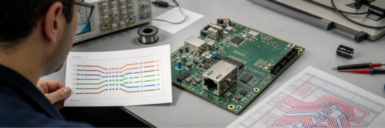
RJ45 Pinout Problems Usually Start at the Jack, Not the Cable
RJ45 pinout work gets risky when connector viewpoint, differential pairs, magnetics, and PoE details stop matching each other on the PCB.

RJ45 pinout work gets risky when connector viewpoint, differential pairs, magnetics, and PoE details stop matching each other on the PCB.
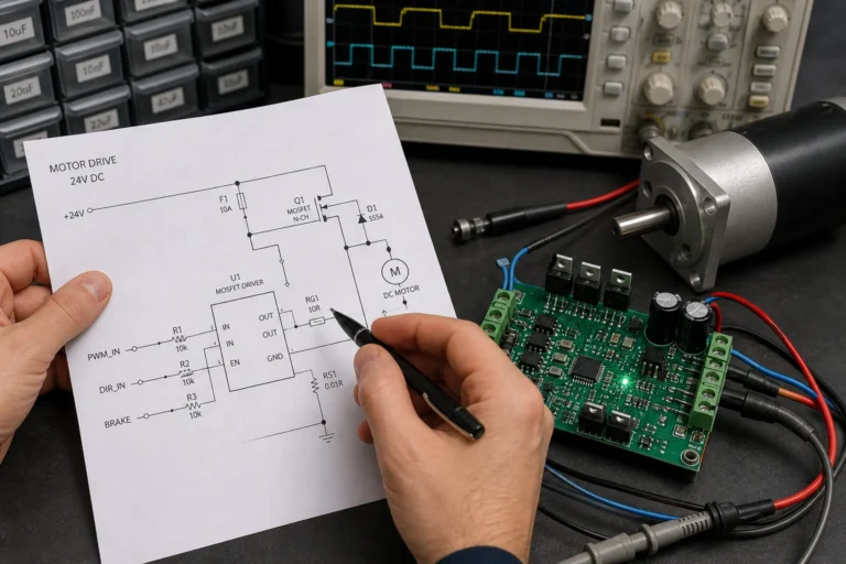
A motor schematic symbol only becomes useful when you read it with the power path, control method, and protection details that surround the load.
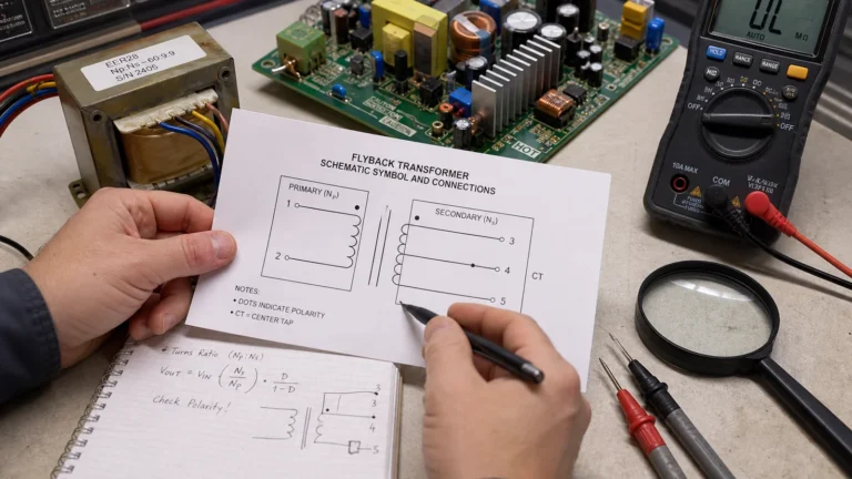
A transformer schematic symbol only helps when it makes winding polarity, taps, isolation, and real circuit intent clear enough for layout, test, and repair work.
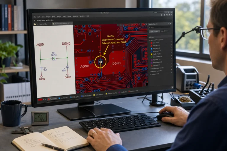
An Altium net tie is useful when two nets must meet at one intentional location without losing their names, rules, or review visibility everywhere else.
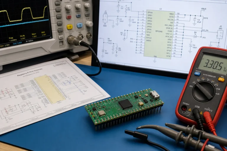
A Pi Pico schematic is most useful when it clarifies the power path, flash boot, USB behavior, and debug access that decide whether an RP2040 board starts cleanly.
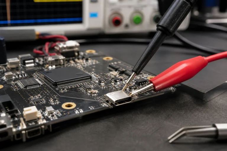
A USB wiring schematic is only useful when it shows connector role, VBUS handling, D plus and D minus routing, shield grounding, and the CC or ID details that affect a real PCB.
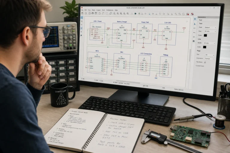
If you want to create a KiCad design from text, start with structured parts, named nets, power assumptions, and ERC checks so the generated schematic stays editable and reviewable.
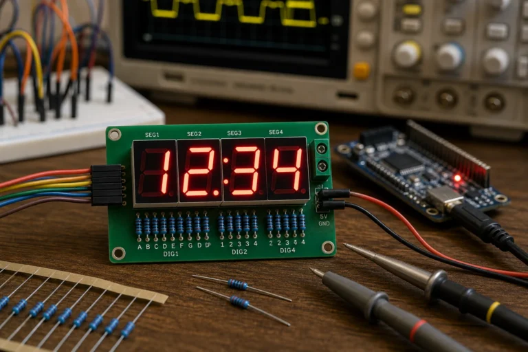
A seven segment indicator is easy to recognize, but the real design work starts with current limiting, common-anode versus common-cathode wiring, multiplex timing, and driver headroom. This guide explains what matters when the display has to work on an actual PCB.

How to make labels in KiCad is really a question about net scope. This guide explains when to use local, global, and hierarchical labels so your schematic stays readable, reviewable, and less likely to hide accidental connections.
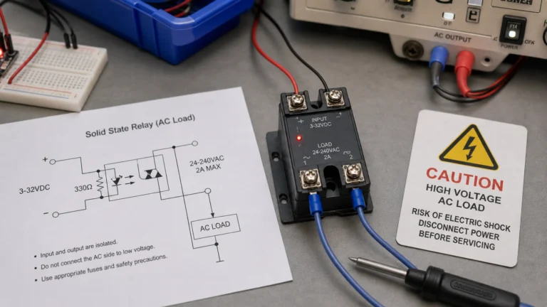
Learn how to read a G3MB-202P solid-state relay schematic, separate input and load sides, and avoid unsafe assumptions when switching AC loads.