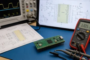
Pi Pico Schematic Checks That Prevent Slow Bring-Up on Custom RP2040 Boards
A Pi Pico schematic is most useful when it clarifies the power path, flash boot, USB behavior, and debug access that decide whether an RP2040 board starts cleanly.

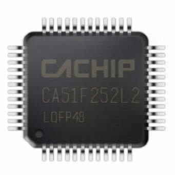


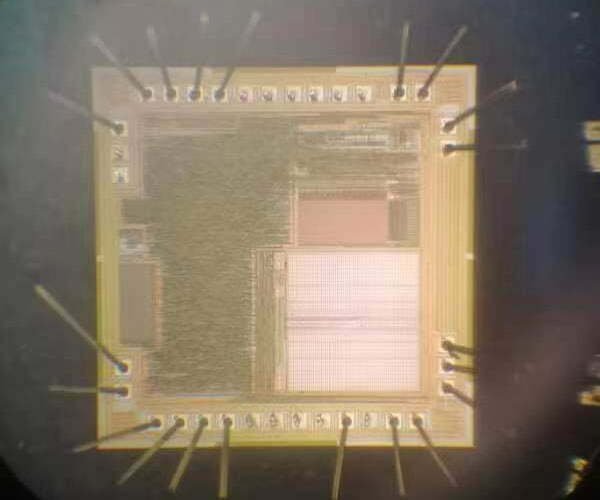
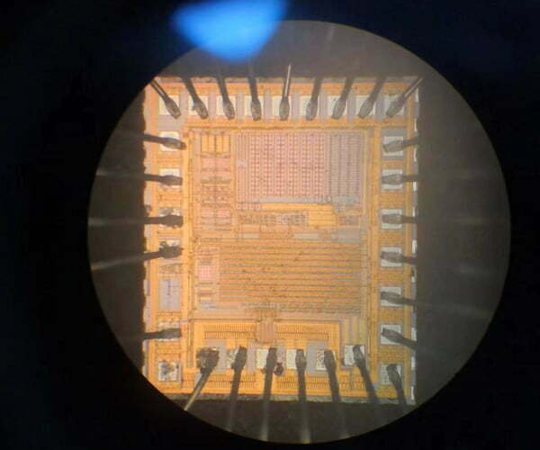
We utilize advanced protocol analysis to identify logical sequences within firmware. By analyzing execution timing and erase sequences in legacy architectures like the ATMEL AT89C series, we identify states where memory becomes accessible. Our team maps firmware structures by detecting data patterns, such as FFFF hex sequences, while assessing the feasibility of recovery or migration to modern hardware platforms.
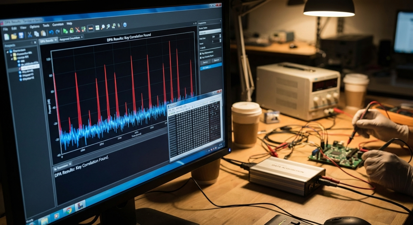
This non-invasive technique monitors power consumption and electromagnetic emissions during chip operation. By applying advanced statistical models, we can infer logic states and execution patterns without physical intrusion. This methodology is crucial for understanding internal device operations and cryptographic processes, providing a deep look into the chip’s functional behavior and data flow.
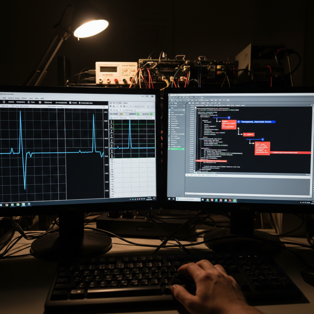
By applying controlled voltage glitches or clock transients, we analyze processor behavior under abnormal operational conditions. This stress methodology helps in identifying hidden design vulnerabilities and improving overall system robustness. It allows engineers to pinpoint critical failure points and reconstruct control flow logic that only emerges during specific environmental fluctuations or hardware exceptions.
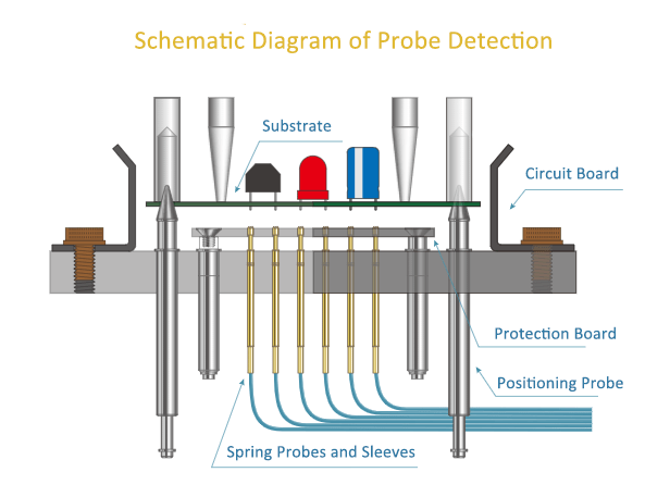
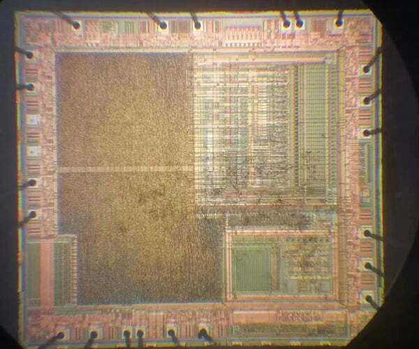
Using high-precision probe stations, we investigate internal wiring and signal behavior in an agreed research or recovery scope. Probing beyond package-level security pins can expose protected internal signals, so any such request requires documented authority covering both the device and the data. Intrusive work can damage the sample and does not guarantee firmware recovery.
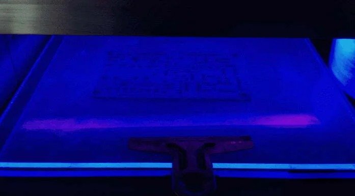
UV exposure can alter or erase stored charge in UV-erasable EPROM devices; it does not reconstruct the original firmware after erasure. Device identification and the preservation of any readable data must precede an authorized assessment. Do not treat UV irradiation as a general recovery method for OTP memory or discontinued industrial chips.
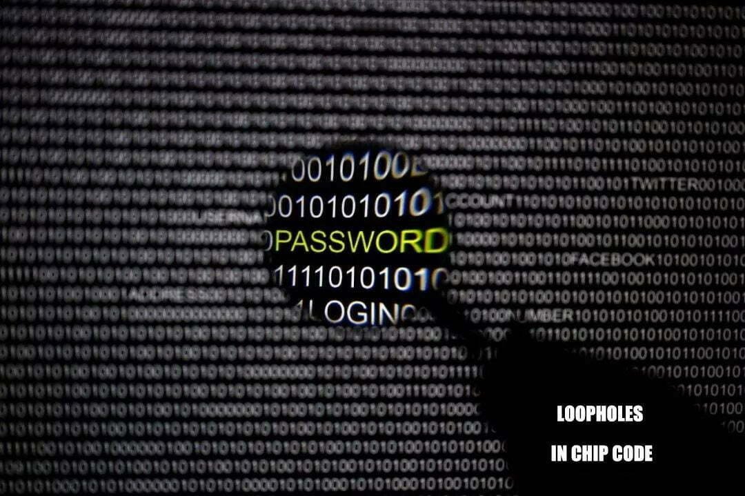
We leverage architectural design characteristics for advanced data recovery. By identifying specific hardware flags or logical flip-flops (FFs) within the memory structure, we evaluate the chip’s state for precise firmware extraction. This methodology is highly effective for the ATMEL 51 (AT89C51) series, where byte-level analysis allows engineers to restore access to critical code lost to hardware obsolescence.
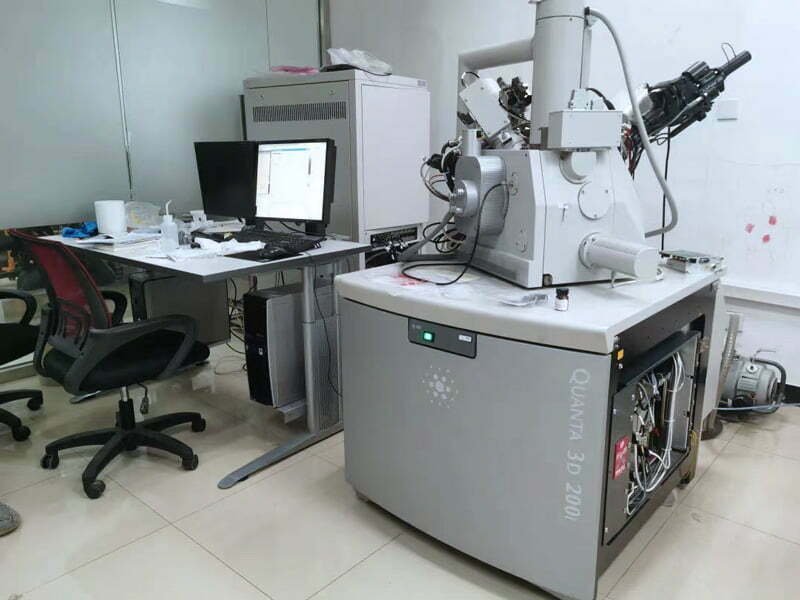
Focused Ion Beam (FIB) technology is our premier method for precision circuit restoration. After chemical decapsulation, we use electron microscopy to modify internal logic paths at the nanometer scale. This is ideal for TI MSP430 series (MSP430F1101A, F149, F425) projects involving security fuses. By restoring circuit states, we enable firmware recovery from protected devices when original source code is unavailable. Requests involving security-fuse modification or protected-firmware recovery require a separate review of authority, device-specific feasibility, and destructive-test consent. A listed chip model is not a promise of access to its code.
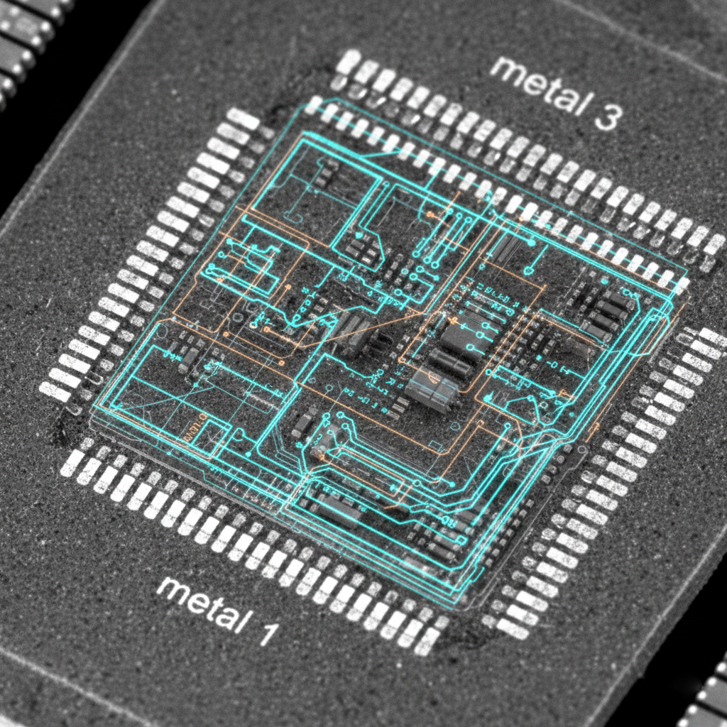
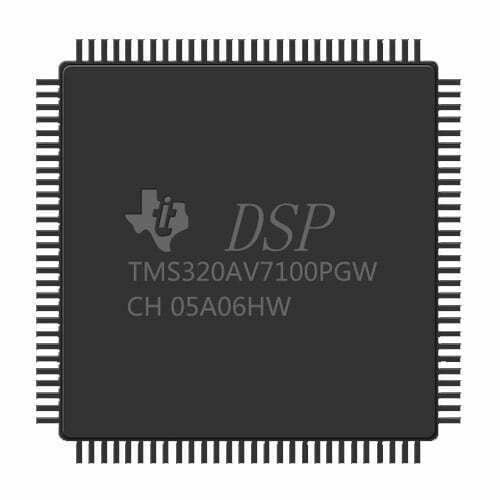
For high-complexity CPLD and DSP chips, we perform deep-level structural analysis to bypass non-functional logic gates and restore access to core system data. This process involves reconstructing complex netlists and identifying hidden signal paths within the silicon fabric. It is particularly effective for the TMS320 series, enabling researchers to recover proprietary processing algorithms for R&D purposes. Any request to access or reproduce proprietary algorithms must include permission from the relevant rights holder and an agreed limit on the use of recovered data.
A Pi Pico schematic is most useful when it clarifies the power path, flash boot, USB behavior, and debug access that decide whether an RP2040 board starts cleanly.
Learn how to choose an EEPROM programmer by package, voltage, interface, clip access, and verification workflow so memory devices are not damaged.
Learn how ESP32 EEPROM-style storage really maps to flash-backed NVS, when to use Preferences, and how to avoid unnecessary flash wear.