What is a JTAG Connector?
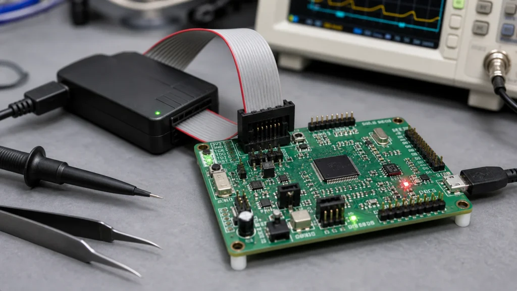
A JTAG connector is a small interface that can make a large difference during firmware development, production testing, and board bring-up. It gives engineers access to a device’s debug and test pins without removing the chip or probing fine-pitch leads by hand. On many embedded boards, the JTAG header is the quiet safety net that helps recover a locked microcontroller, program flash, or inspect hardware faults.

JTAG stands for Joint Test Action Group, but in daily engineering work the term usually refers to a debug/test interface using signals such as TCK, TMS, TDI, TDO, reset, voltage reference, and ground. The exact connector style varies by device family and toolchain, so a “JTAG connector” is less a single universal part and more a design choice that must match the target chip and debugger.
What a JTAG Connector Is Used For
JTAG can support boundary scan, programming, debugging, and production test. Boundary scan checks interconnects between chips without needing physical access to every net. Debugging allows breakpoints, register inspection, memory reads, and firmware stepping. Programming can load bootloaders or production firmware. In manufacturing, JTAG can help verify that the printed circuit board assembly is alive before full functional testing.
Not every product needs a permanent populated header. Some boards use test pads, tag-connect footprints, or unpopulated pin headers to save space and cost. The right choice depends on whether the interface is for lab development, factory programming, field service, or failure analysis.
Common JTAG Signals
The basic JTAG signals are TCK, TMS, TDI, and TDO. TCK is the test clock. TMS controls the test state machine. TDI carries data into the target device. TDO carries data out. Many designs also include TRST or system reset, a voltage reference pin, and several ground pins.
Voltage reference is easy to overlook. A debugger often needs to know the target I/O voltage so it can drive the interface safely. If the connector omits VTREF, the debug tool may not connect reliably, or worse, it may drive the wrong voltage into the target.
Pinout Is Not Universal
There are common JTAG header layouts, including 10-pin and 20-pin ARM-style connectors, but engineers should not assume pin compatibility. ARM Cortex debug headers, FPGA JTAG headers, legacy 20-pin connectors, and vendor-specific layouts may use different pin assignments and keying.
Always check the target device reference manual and debugger documentation. A connector that “looks right” can still swap TDI and TDO, miss reset, or place voltage reference on the wrong pin. Clear pin-1 marking on the silkscreen is also important because reversed cables are a common bring-up mistake.
PCB Layout Tips
Keep JTAG traces reasonably short and direct. They are not usually high-speed RF signals, but long stubs, noisy routing, or poor grounding can cause intermittent debug failures. Route TCK with care because it is the clock. Place ground near the signal pins in the connector, and avoid running the debug interface through noisy switching areas when possible.
If the connector is near the board edge, make sure the cable can plug in when the product is assembled. Mechanical access matters as much as the schematic. Good PCB layout guidelines include service access, connector orientation, and test fixture clearance, not only electrical routing.
Pull Resistors and Reset
Some JTAG pins need defined idle states. Pull-ups or pull-downs may be recommended by the chip vendor, especially for TMS, reset, boot mode pins, or debug enable pins. Do not add strong pulls blindly; they can fight the debugger or affect boot behavior.
Reset routing also deserves attention. A debugger may need to reset the target to halt early boot code. If reset is not available, connection may still work, but recovery from bad firmware can be harder.
Production and Security Considerations
Leaving JTAG accessible is useful for manufacturing and service, but it can be a security risk in finished products. Attackers may use an exposed debug interface to read firmware, alter memory, or bypass protections if the device is not locked.
For production boards, decide how JTAG should be handled after programming. Options include firmware debug lock bits, depopulated headers, hidden test pads, access-controlled service fixtures, or epoxy in high-risk products. The decision should be part of the product’s PCB design service review, not an afterthought at release.
Troubleshooting JTAG Connection Problems
If a debugger cannot connect, check target power first. Then verify ground, VTREF, pin orientation, reset behavior, and whether the chip is held in the correct boot mode. Slow down the JTAG clock during initial bring-up. Inspect solder joints on the connector and confirm that TDI and TDO are not swapped.
On a new board, compare the schematic symbol, footprint, cable orientation, and debugger pinout side by side. Many JTAG issues are not deep silicon problems. They are simple mapping errors between the cable and the board.
Bottom Line
A JTAG connector is a small feature that can save hours during firmware and hardware debugging. Choose the pinout deliberately, mark it clearly, route it cleanly, and decide how it should be secured in production. When designed well, it becomes one of the most useful access points on an embedded PCB.
What is a JTAG connector used for?
A JTAG connector provides access to debug, programming, boundary scan, or production test signals on a PCB. Typical signals include TCK, TMS, TDI, TDO, reset, reference voltage, and ground.
Why does pin 1 orientation matter on JTAG?
Many JTAG cables are keyed or marked around pin 1. Reversing the cable can connect signals to the wrong pins, which may stop programming or, in poorly protected designs, damage the target.
Should every board include a JTAG connector?
Not necessarily. Some products use pads, pogo-pin fixtures, or a smaller programming header. The right choice depends on production volume, enclosure access, debug needs, and available PCB space.