RJ45 pinout questions often look simple until the design moves from a cable diagram to a real PCB. On the bench, the expensive mistakes usually come from mixing plug-view and jack-view numbering, crossing differential pairs at the magnetics, or assuming a PoE center tap behaves like a casual spare pin. The color order is the easy part.
This guide focuses on the version of RJ45 pinout that matters in engineering work: how T568A and T568B map into Ethernet pairs, how those pairs appear at the connector and magnetics, and what to verify before layout, bring-up, or field repair.
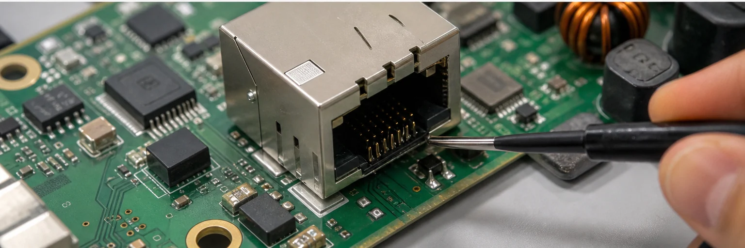
Start with the pair assignment, not the wire colors
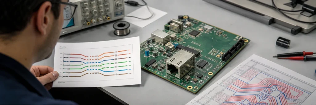
The practical heart of an RJ45 pinout is the pair map. For Ethernet, pins 1 and 2 are one differential pair, pins 3 and 6 are another, pins 4 and 5 form a pair, and pins 7 and 8 form the last pair. T568A and T568B mainly swap the green and orange pair positions. They do not change the fact that the PHY, magnetics, common-mode chokes, and cable all expect twisted pairs to stay paired.
That distinction matters because PCB errors usually do not come from using A instead of B. They come from breaking pair integrity when the footprint, integrated-magnetics jack, or schematic symbol is interpreted from the wrong side. A harness technician may care about conductor color. A PCB designer should care first about pair continuity, polarity, and return path consistency.
- T568B pair order: pins 1-2 orange pair, pins 3-6 green pair, pins 4-5 blue pair, pins 7-8 brown pair.
- T568A pair order: pins 1-2 green pair, pins 3-6 orange pair, pins 4-5 blue pair, pins 7-8 brown pair.
- Engineering takeaway: as long as both ends match the intended standard, the board still lives or dies on pair routing discipline, not on memorizing jacket colors.
Why connector numbering causes more trouble than the standard itself
Many design reviews fail because the symbol, footprint, and mechanical drawing do not all show the same viewpoint. Some connector datasheets show the mating face. Others show the PCB solder side. Integrated jacks may add shield tabs, LEDs, transformer pins, and center taps on separate numbering systems. If the team assumes the image is a front view when it is actually a bottom view, the final board can swap pairs even though the schematic looked tidy.
A safe workflow is to annotate the schematic symbol with the viewpoint, then cross-check the footprint against the datasheet pin table before routing starts. For magnetics-integrated jacks, verify three things separately: cable-side pair pins, transformer-side PHY pins, and any LED or shield tabs. Those non-signal pins are easy to misplace when the connector body is crowded.
This is also where DFT and repair reality show up. A misplaced LED pin is annoying. A swapped pair inside an integrated jack section can waste hours because link LEDs may still behave partially normally while autonegotiation or PoE classification fails.
How the RJ45 pinout changes once PoE is involved
When Power over Ethernet enters the design, RJ45 pinout work stops being only a data-pair exercise. Depending on the PoE mode and the PD or PSE architecture, power can be delivered over the data pairs or the spare pairs through center taps and bridge circuitry. That means the connector region now carries surge exposure, isolation requirements, current handling, and thermal consequences in addition to signal integrity.
On a PCB, that pushes the review beyond “are the eight pins in the right order?” The better questions are these: where do the center taps land, where is surge protection placed relative to the connector, how is chassis or shield termination handled, and does the copper around the power path stay sensible under current and temperature rise? A correct cable pinout will not save a board whose PoE entry path forces noisy or overstressed routing.
- Check center-tap intent. Do not leave transformer center taps floating by assumption; confirm whether they feed bias, Bob Smith termination, PoE power extraction, or shield-related networks.
- Check creepage and isolation. Connector-adjacent magnetics and PoE circuitry should respect the isolation barrier shown by the jack or transformer datasheet.
- Check thermal and surge path. TVS placement, return path length, and copper neck-downs can matter more than the nominal pinout table once field transients arrive.
Layout rules that keep a correct pinout from failing on the board
Even when the RJ45 pin map is correct, layout can still undermine Ethernet performance. Differential pairs should stay coupled and length-aware between the PHY and magnetics, and the connector escape should avoid needless stubs or layer changes near the jack. If integrated magnetics are used, the layout burden shifts toward the transformer-to-PHY side, shield treatment, and any PoE or LED support pins.
Designers also need to resist decorative routing. There is no value in crossing pairs on the PCB just to make the connector pin sequence look visually neat in the layout editor. Let the electrical pairing drive the geometry. On fast boards, that usually means controlled return paths, minimal asymmetry at pair breakouts, and clean separation between noisy power entry structures and the Ethernet analog front end.
If the product has to survive compliance work or noisy industrial environments, connector placement matters too. A long exposed run from the jack to surge components gives ESD and EFT energy more board area to disturb. Placing protection and chassis-related structures with intention often matters more than any single routing tweak deeper in the board.
What to verify during bring-up and troubleshooting
When a new board does not link correctly, start with the RJ45 pinout evidence chain instead of jumping straight to the PHY register dump. Confirm the jack part number, the intended T568 scheme, the schematic symbol mapping, the footprint orientation, and continuity from connector pins through the magnetics path. A simple continuity check is often enough to catch a swapped pair, misread viewpoint, or assembly-side connector rotation.
After that, move to signal-level checks: transformer center taps, link pulse presence, LED behavior, and PoE classification if the design uses powered Ethernet. Field failures also deserve a mechanical look. RJ45 jacks see insertion wear, cracked shield tabs, marginal solder on side stakes, and lifted pads when the enclosure transfers stress into the connector body. Those are repair issues, but they often masquerade as a pinout or firmware problem.
Common RJ45 pinout mistakes on PCB projects
The repeat offenders are familiar:
- Confusing plug view with jack view. The pin sequence is mirrored and the board ends up with crossed pairs.
- Treating pins as individual conductors instead of differential pairs. The number table looks correct, but pair integrity is broken around the magnetics or PHY.
- Ignoring the extra pins on integrated jacks. LEDs, shield tabs, and center taps are not interchangeable with signal pins.
- Forgetting PoE consequences. A board can pass a casual continuity check yet still fail under surge, thermal load, or classification behavior.
- Skipping assembly inspection around the connector. Large stake tabs and dense front-edge routing make solder escapes and hidden cracks more likely than many teams expect.
Use the pinout as a system check, not a memorization test
A correct RJ45 pinout is only the starting point. In real PCB work, the useful question is whether the pair map, connector viewpoint, magnetics path, PoE network, shield strategy, and inspection plan all agree with each other. If they do, the board is usually easy to route, test, and repair. If they do not, even a familiar Ethernet connector can create a surprisingly expensive debug cycle.
What is the standard RJ45 pinout for Ethernet?
For Ethernet cabling, the standard pair positions are pins 1-2, 3-6, 4-5, and 7-8. T568A and T568B mainly swap which color pair occupies pins 1-2 versus 3-6.
What is the most common RJ45 pinout mistake on a PCB?
The most common mistake is mixing plug-view and jack-view numbering, which can mirror the connector and swap differential pairs even when the schematic seems correct.
Does PoE change how I should review an RJ45 pinout?
Yes. Once PoE is involved, you also need to verify center taps, surge protection placement, isolation spacing, shield treatment, and current-handling paths near the connector.
Is T568A better than T568B for PCB design?
Neither is inherently better for the PCB. What matters is matching the intended cable standard and preserving pair integrity from the connector through the magnetics and PHY.