The Basics of Low Noise Amplifiers
A low noise amplifier (LNA) is a type of electronic amplifier used to amplify signals with very low noise. It is an essential component used
Schematic & Gerber restoration
MCU/CPLD code restore access & backup
1:1 exact hardware replication
BLE & Classic BT wireless solutions
Precision PID & thermal management
High-efficiency motor drive control
Industrial RS485/RTU communication
Custom STM32/ESP32 firmware & HW
Calculate the PCB trace width based on temperature rise, current, and copper thickness (IPC-2152).
Reverse-engineering old PCBs for schematics? It’s often a tedious, time-consuming task.
That’s where Well Done Company comes in—our team’s expertise and experience ensure you complete the process easily and precisely.
Trusted By
Established in 2008, Well Done Technology focuses on PCB reverse engineering, PCB clone, and IC unlock. Our technical team of more than 40 people includes senior engineers with rich experience. With 13 years of practical experience, we have completed over 1000 pcb engineering for clients worldwide, including North America, Europe Southeast Asia.
Looking for more service about PCB engineering? Your can benift from our wide range of services as below. And our experts will ensure no delays due to quality or errors while working on your project.
When designing a PCB stackup, we can help our customers guide, create or verify the stackup. They are suitable for all impedance control requirements for single-ended, differential pair, coplanar waveguide and other technologies.
Due to the growing application of low-impedance circuits, low-impedance modeling has become an important aspect of circuit design. If you have mpedance-controlled requirements, we can help you for controlled impedance modeling.
Design Rule Check verifies trace and space, open or shorted nets, aspect ratio, and other parameters of your design. It's used to prevent potential errors in the production process by identifying them in the design phase.
There are numerous printed circuit board surface finishes, including ENIG, HASL (Tin-lead or lead-free), Immersion Silver, ENEPIG, and so forth. Well Done has rich experience assisting customers in choosing the correct surface finish solution.
Gerber files are generally more accurate than DXF files since they are meant for machine-readable output. You can use a variety of software programs to convert DXF to Gerbers. Some of the most popular programs include: Gerbv, Adobe Illustrator, CorelDRAW.
High Density Surface Mount Technology (HD-SMT) uses very densely packed arrays of small, closely spaced pads. This enables significantly higher component density than traditional surface-mount.
Found in 2008, Well Done PCB Limited is a circuit board engineering company in China. We provides excellent PCB engineering services by combining innovative solutions with high standard. We are dedicated to realize electronic product reduction and clone services for everyone. No matter how difficult your PCB project is, we can tailor and customize it for you.
Well Done Technology was founded by Xia and Lee in 2008, is a leading PCB reverse engineering firm in China. We focused on PCB cloning, reverse engineering, and chips unlock services.
By 2012, our team expanded to over 50 members, including 5 senior technicians. To meet the client demands, we made a strategic shift to prioritize reverse engineering as our core business.
In 2017, we successfully penetrated global markets, with over 50% of clients originating from international regions. We had completed more than 1,000 PCB reverse-engineering projects.
In 2022, we launched the expansion of our laboratory base and the comprehensive upgrade of high-tech electronic equipment, aiming to improve the efficiency of our service to customers.
More than 15 years of experience in pcb engineering;
Authoritative computer aided engineer degree;
Well-received cooperation cases;
Focus on reverse engineering;
Rapid electrical test and repair;
Experienced in pcb design and development;
RF, high-speed circuits;
Industrial control, analog, digital;
Microchip, semiconductors;
Multi-layers PCBs (4 layer, 6-layer, 8 layer, and 10 layer);
Single sided, double sided;
Rigid and flexible pcb;
PCB engineering evalue and suggestion;
Affordable and neogiationable prices;
Signing the contract with non-disclosure agreement;
One-to-one expert service;
Formal email & phone call back;
Response within 24 hours;


A low noise amplifier (LNA) is a type of electronic amplifier used to amplify signals with very low noise. It is an essential component used

In recent years, the redistribution layer (RDL) technology has gained significant traction. It’s a revolutionary packaging solution that has transformed the way we package ICs.

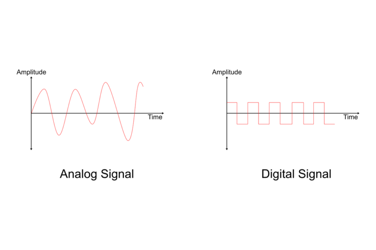
When you tune the radio in your car or home, you are listening to different types of signals. You may not think about it much,

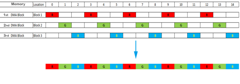
This article aims to introduce the application of DMA2D mode through the STM32H563 development board. The so-called DMA 2D mode means that the DMA can
Please provide high-definition pictures of both sides of the circuit board, the number of layers, the size and details of any encryption chips.
For damaged circuit boards where the original manufacturer has discontinued production, we assist in reverse engineering the board through methods such as comparing manufacturer data sheets, circuit logic analysis, and X-ray imaging technology. However, we cannot guarantee 100% consistency with the original board.
Yes, we provide software reverse research and development services: software program code extraction, software rewriting, software secondary development, software disassembly, software system modification and upgrade, etc.
We can do IC reverse engineering or decryption for STMicroelectronics, Xilinx, Altera, Lattice, Atmel, Microchip, Actel and more. You can find more details at Supportable IC Series & Models.
Yes, our self-developed PCB copy board software can truly achieve 100% cloning without any mistakes. We can send these electronic files to you: standardized PCB files, schematic diagrams SCH and BOM and other materials.
In generally, it’ll takes 5–7 business days for single/Layer boards, 10–15 business days for Multi-Layer (2–16 layers) boards, and 15–20 business days for high-density/advanced tech (HDI, Flex PCBs).
Absolutely. We can redesign your PCB such as upgrading components for availability/cost, reducing board size, improving thermal performance, or enhancing signal integrity.
Our engineers specialize in Altium Designer, KiCad and Cadence OrCAD. We provide files in industry-standard formats (Gerber, ODB++, BOM, schematic PDFs).
We offer rapid prototyping and test (AOI & ICT). Material options: FR-4, Rogers, aluminum-based PCBs, and flexible circuits.
We provide services for medical devices, industrial electronics, consumer electronics, IoT & embedded systems, etc.
Send us a message if you have any questions or request a quote. Our experts will give you a reply within 24 hours and help you select the right bits you.
We respect your privacy and have a strict Privacy Policy to protect your personal information.