PCB designers need to understand PCB trace basics to create high-performance printed circuit boards. From basic definitions to the types of traces, this article covers all the fundamentals you need. Working with printed circuit board (PCB) design software can be challenging at times. That’s because many technical terms and acronyms may seem confusing at first glance. Even if you’ve never worked with PCB design software before, it won’t take long for you to get comfortable with it. This blog post will explain some of the more basic concepts that are essential for understanding PCB designs and working with them effectively.
What is PCB Trace?
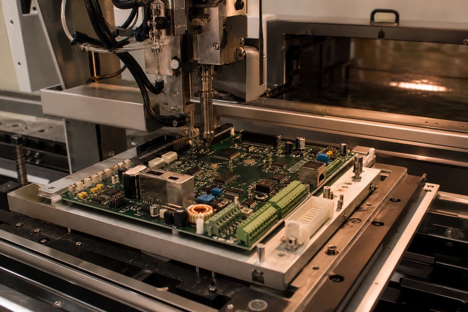
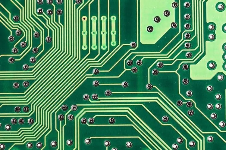
A printed circuit board trace is a path on a printed circuit board that connects two points. Trace is the most fundamental component in PCB design and pcb reverse engineering. A trace may be a single line or a grouping of parallel lines. It may be on the top layer or buried inside the board. Trace is used to connecting components on a printed circuit board. To understand trace usage, it’s helpful to have an idea of what a printed circuit board is used for.
PCB trace width
The trace width is the width of the trace itself, not including the width of any copper pour above or below it. It is one of the most important specifications for a trace, mainly because it will affect the current that flows through the trace. The unit of trace width is usually millimeters (mm). In the PCB design software, you’ll need to input the trace width in pixels to see the final traces. If you don’t, the software will assume that you are using a 10 mil trace width, which is a very common value.

How to Calculate PCB Trace Width?

While this formula highlights how width directly impacts resistance, manual calculations can be tedious. Skip the hassle—explore our calculator to let smart algorithms handle the math, ensuring low resistance and optimal trace width in seconds.
PCB trace length
Trace length is the distance between the start terminal of a trace and the end terminal of the trace. The trace length can affect a few things with your PCB design, including maximum current capacity and the length of the trace itself. To calculate the trace length, you need to know the current that you want to flow through the trace to determine the trace length.
The maximum current capacity will help you find the length at which the trace begins to overheat and become unreliable. You can also use this formula to determine the trace length: L = I / C where L is the trace length, I is current, and C is the capacitance of the trace itself.
PCB trace thickness
The trace thickness (also known as the copper pour thickness) is the width of the copper on the PCB. As you can imagine, trace thickness can greatly affect the current capacity of a trace. In most cases, the trace thickness is found by adding the trace width and the clearance of the board. It’s important to take the clearance of the board into account because this will reduce the current capacity of the trace. Tracing is the process of applying a conductive material like copper to a substrate. The substrate might be a printed circuit board, a conductive coating applied to a substrate or even a conductive adhesive.
PCB trace spacing
The trace spacing is the distance between the traces on your PCB. It will affect trace width and how much current each trace can handlethe. This is because the trace width is usually determined by the copper pour width, which is the width of the copper between the traces. If the trace spacing is too wide, the copper pour will be wider than the trace. This will result in a wider trace width, which isn’t always a good thing. You can use this equation to determine the trace spacing: S = W – 2 × T where S is the trace spacing, W is the trace width, T is the trace thickness, and 2 is the trace clearance.
PCB trace orientation and solderability
The trace orientation is the direction that the traces are running on the PCB. It will also determine the solderability and impedance of your PCB. Impedance is a measure of how much current is slowed down by the PCB. The trace orientation and solderability of the traces can be controlled by the copper poured around the traces. If the copper pour is close enough to the traces, it can affect their orientation and solderability.
PCB Trace Material Selection
When it comes to selecting the right material for your PCB trace, there are a few key factors to consider:
- First, the level of current. If you are carrying high currents, then you will need to select a material with good conductivity. Copper is a good choice for high current applications.
- Second,the trace width. The wider the trace, the more current it can carry.
- Third, the impedance of the trace. This is important for high-speed applications where signal integrity is critical.
- Fourth, the amount of heat. If the trace will be carrying high currents or will be operating at high speeds, then you will need to select a material that can dissipate heat effectively.
- Finally, the cost of the material. Copper is the most expensive option, but it is also the most versatile.
PCB via size
Remember that a trace isn’t just the copper lines on a PCB. The trace also has an “electrical” connection to the rest of the board, typically in the form of a via. A via is how a trace on one layer of a PCB is connected to a trace on another layer of the PCB. Thus, the via is the connection point between the two layers of the PCB. Via size is determined by the current that flows through the via. This can be tricky because it’s not as straightforward as it is with a trace. To determine the via size, you need to take the capacitance and inductance of the via into account. The capacitance and inductance of the via are affected by the copper thickness, copper pour size, and via hole size. Via hole size is the diameter of the via hole that is drilled through the PCB.

Conclusion
PCB trace is the most fundamental component of PCB design. A trace is a path on a PCB that connects two points to connect components. The trace is on the top layer or buried inside the board. Trace width, length, and thickness are important considerations when designing PCB traces. Keep these trace basics in mind when designing your PCB. This will help you create high-performance printed circuit boards.