PCB Clone
What is PCB Clone?

PCB Clone, also called pcb duplication, is the process of creating a copy of the original PCB using reversely researching method in electronic industry. This is useful when you have multiple versions of the same printed circuit board, or if you need to create new products that use the same PCB design. You might also clone a PCB to reuse parts from an existing printed circuit board for another project. If you are new to electronics and don’t know how to clone a PCB, we will give you essential information on everything you need to know about cloning printed circuit boards.
Why You Need PCB Clone Service?
PCB copying is a cost effective way to make multiple copies in pcb production process. You may need to make multiple boards for product testing, create a few sample boards for customers, or you may be building boards for mass production. In each case, cloning the PCB can easily create the desired number of boards with minimal effort. Additionally, if you have an old design that is no longer available, you can clone the PCB to create new boards from the old design. Below are all benefits that you can get from our pcb cloning service:
Make changes or improvements to the original design;Create multiple copies of a PCB for mass production;Make an identical copy of an existing electronic product;Make a PCB with modifications from an existing PCB;Create a PCB from a design;Make a backup in case the original is lost or damaged;Test a design before manufacturing;Fix damaged tracks;Replace missing electronic components;
How to Clone a PCB Board?
There are a few different ways to clone a printed circuit board. Each method has its own benefits and drawbacks. Make sure you understand the process and potential pitfalls of each method before choosing a technique. This will help you make an informed decision and produce the desired results. Generally, we’ll clone pcbs according below procedures:
Tips:
For #1, IC unlock is only necessory only if your program is locked.
For #2, it’s the most important process. You need to get the bill of material bom and schematic diagram by using reverse engineering technology.
Required tools and equipment:
- Computer
- AUTOCAD
- Scanner
- PORTEL
Step 1: Scan the original PCB
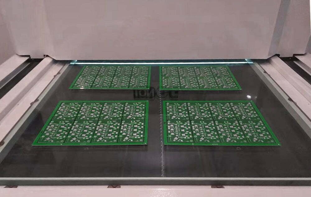
First, you must put the original PCB inside the scanner. And then, you must adjust the scanner’s contrast and brightness settings.

Step 2: Open AUTOCAD and create a file
To begin, open AUTOCAD and create a file. From the insert menu, select raster images. Then, select the desired image for the project. The insert image box will appear. When you insert an image, draw a rectangular frame around the PCB. Use the object lock point as much as possible when building the structure to ensure tracking.
Step 3: Drawing component package and the shape
To begin, create a board design by calculating the quantity of boards in the design. Every package must include one board drawing. After that, use PORTE99 to generate the electronic components package and shape.
Step 4: Put the CAD file to PRORTE99
Open the PORTEL99 PCB editor and select ‘import CAD file’ from its menu to create a new PCB file. Import the CAD file into it. Once you import it, you will see the component packaging graph in the PORTEL99 editor.
Step 5: Create another PCB component editor
PROTEL99 provides a PCB component editor where you can open another one and place a component.
Step 6: Send the component packages to CAD File
After you have finished creating all the component packages in the PROTEL99 editor, send each one to a CAD file.
Step 7: Copy the component package to the CAD
Make a copy of the PCB image into the imported CAD file by duplicating the newly created CAD file’s component package. Open both CAD files.
Step 8: Put the vias and pads
Measure the inner, external, and internal diameters of the pads and vias, then choose the Circle sub-item from the drawing menu. After that, you must compute the ring’s inner and outer dimensions. You will not be able to place both the square and polygon pads because of this. Furthermore, you must place each pad based on its size. Fill in the CAD instead.

Step 9: draw the trace and put the silkscreen
At the end, you can use the Drawing menu to select the line aggregate. Then, you can add the silkscreen. If you want an irregular screen, you must use the polymer line.
Is PCB Clone Legal?
PCB cloning is a legal process, as long as the original board was created legally. This means that if you have purchased a board and have the legal right to modify and reproduce it, then you can clone the board. However, if you are trying to clone a board that you do not have the legal right to modify or reproduce, then you may be breaking the law.
