PCB Design Cases

Counterbore vs Countersink
What is a Counterbore? A counterbore, on the other hand, is a cylindrical hole with a flat bottom, typically consisting of two parts: a larger diameter top section and a
Mastering PCB Beveling: Techniques, Tools, and Best Practices
In the intricate world of printed circuit board (PCB) manufacturing, precision and quality are paramount. One critical aspect that significantly impacts the performance, durability, and aesthetics of PCBs is edge
Common PCB Design Problem
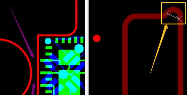
PCB Design Issues Drilling Hole Problem:Irregular hole ring design Risk:May confuse hole attributes Recommendation:Hole ring should be a hollow ring Problem:Holes without wire connections Risk:May lead to incorrect hole attributes

PCB Vias: Types & Design Best Practices
Learn via types: through-hole, blind, buried, and vias-in-pad. Tips for spacing, drilling, and reliability in multi-layer PCBs. Essential for advanced layouts. Guide inside!
Auto Place and Route with Altium Designer
When designing a PCB, in order to improve efficiency, we need to learn how to automatically place and route our projects. In this tutorial, we will introduce the auto place
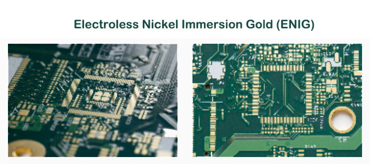
ENIG Surface Finish: PCB Design Guide
ENIG (Electroless Nickel Immersion Gold) basics: thickness, pros/cons, and applications. Learn to specify ENIG for lead-free PCBs. Best practices inside!
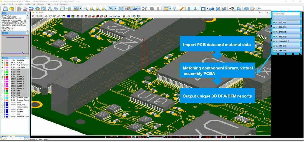
Mastering Design for Manufacturing (DFM)
What is DFM? Design for Manufacturing (DFM) is actually a bridge between R&D and production. It simplifies, optimizes, and improves product design to produce better products at a lower cost.
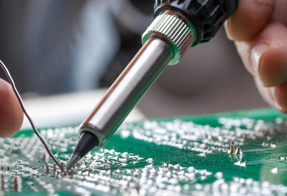
Wicking Solder: How to Prevent & Fix?
Learn to avoid solder wicking: causes (overheating, poor flux), prevention tips, and repair methods. Essential for clean PCB soldering. Step-by-step guide!
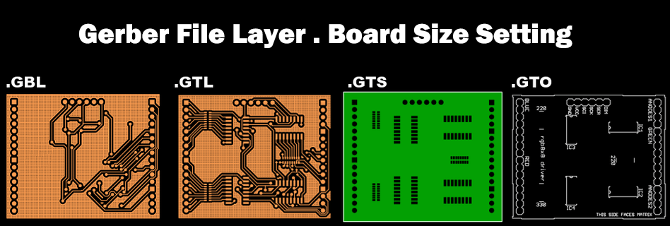
Gerber Files Board Size Setting
Are you struggling with creating Gerber files for your PCB projects? The process of designing and producing printed circuit boards can be challenging, especially when it comes to getting the

140 Commonly Used PCB Markings
Printed circuit boards, or PCBs, are a vital component of electronic devices, as they provide a platform for electrical components to be connected and communicate. To ensure that the PCBs
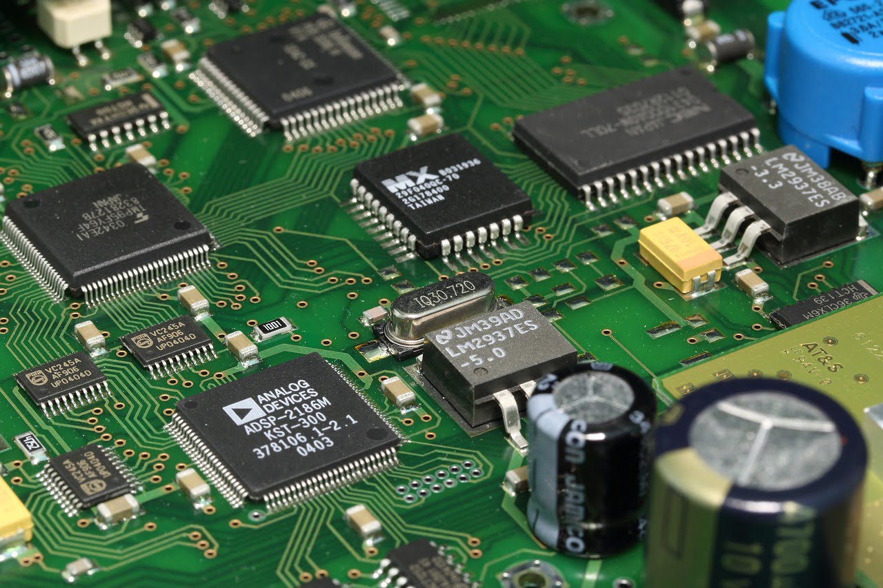
Cool Your PCBs with These Easy Cooling Techniques!
As a hardware engineer, I understand the importance of cooling Printed Circuit Boards (PCBs) for optimal performance. Without proper cooling, your PCBs can suffer from a range of issues like
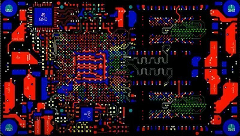
Design High Speed PCBs: Tips and Strategies
Design high-speed PCBs: impedance control, layer stacking, and crosstalk mitigation. Tools and strategies for 5G, USB 3.0, and HDMI layouts. Expert guide here!
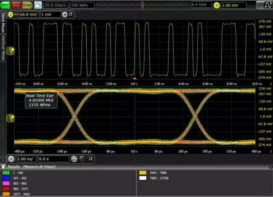
Signal Integrity Analysis in High Speed PCB Design
Master SI issues: reflections, crosstalk, and impedance control. Tips for routing, termination, and simulation tools like HyperLynx. Critical for high-speed designs!
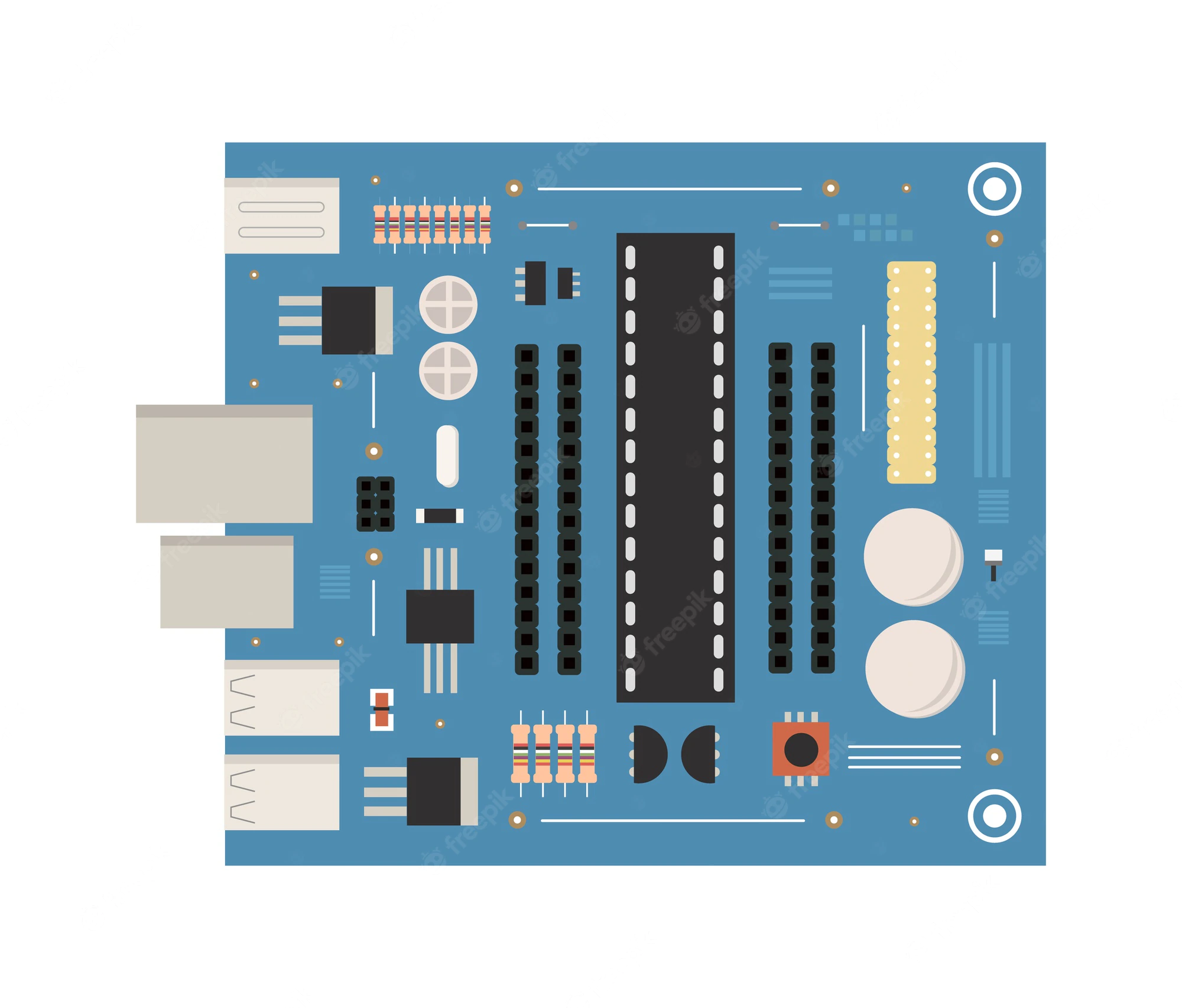
Through Hole vs Surface Mount
How many do you know about through hole vs surface mount? They are two ways to connect electronics components in pcb assembly (PCBA). They are cost-effective and reliable methods of

How to Create a PCB Library: Step-by-Step
Build PCB libraries: component footprints, symbols, and 3D models. Tools for Altium/KiCad and version control. Essential for efficient design. Tutorial inside!
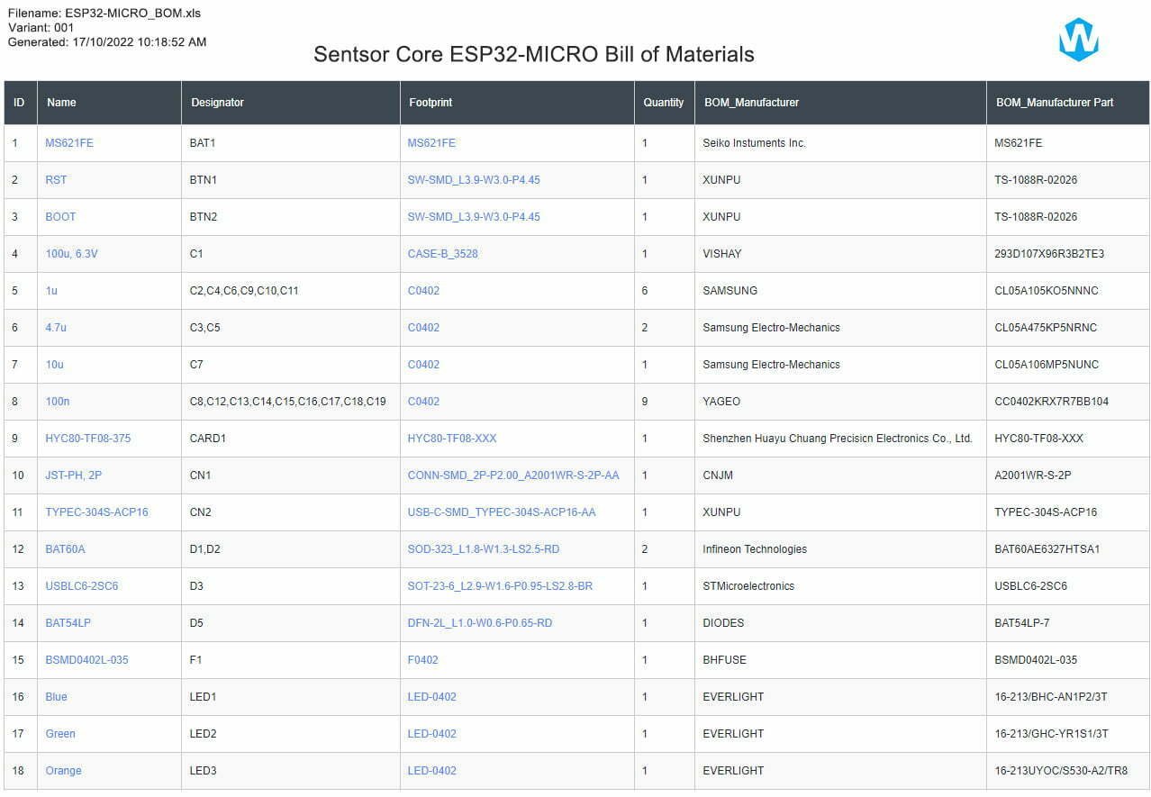
How to Create a PCB BOM: Step-by-Step Guide
Master PCB BOM creation: component listing, part numbers, and sourcing. Tips for accuracy, cost optimization, and manufacturability. Download template inside!

Effective PCB Footprint Strategies
What is PCB Footprint? PCB footprint, is the arrangement of pads used to mount a specific component to a printed circuit board. The footprint defines the outline of the component

PCB Layout Guidelines For A Successful Design
Master PCB layout: trace width, ground planes, and component placement. Tips for signal integrity, thermal management, and manufacturability.

5G PCB Manufacturing: The Next Generation of Mobile Connectivity
The adoption and implementation of 5G connectivity are underway, as mobile carriers race to be the first company with a 5G network. A key enabler of 5G is low latency,
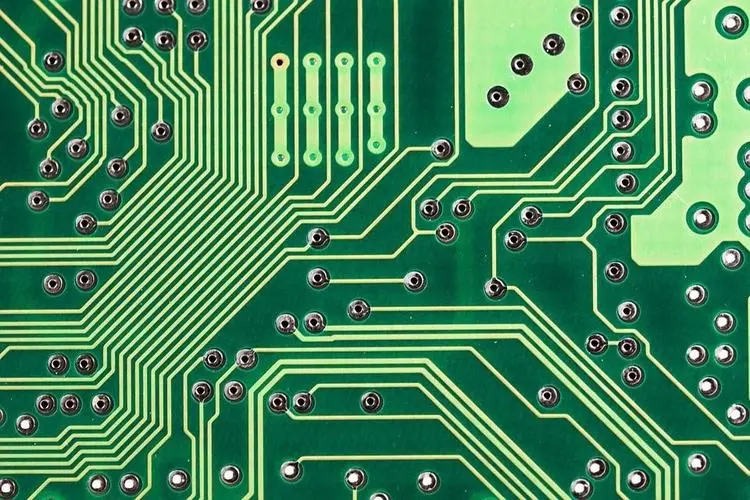
PCB Trace Basics for PCB Designers
PCB designers need to understand PCB trace basics to create high-performance printed circuit boards. From basic definitions to the types of traces, this article covers all the fundamentals you need.
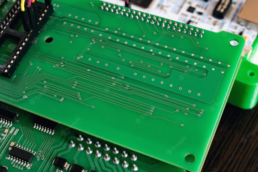
PCB Stackup Design: Beginner’s Guide
New to stackups? Learn layer configuration, dielectric materials, and impedance control. Tips for multi-layer PCBs and signal integrity. Step-by-step inside!
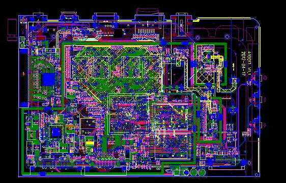
6 Layer PCB Manufacturing Process: The Complete Guide For PCB Designers and Manufacturers
What is 6-Layer PCB Manufacturing? 6-layer PCB manufacturing is the mass-production of PCBs with a minimum of six layers. In a 6-layer PCB, the top and bottom layers are usually

How to Solder Wires to a Circuit Board?
When building a circuit, you’ll often need to connect circuit board components together. Soldering wires to a circuit board is a basic technique for making connections between components. NOTE: Soldering

How Much Does PCB Prototyping Cost?
The total cost of an electronic product prototype usually includes the cost of the printed circuit board (PCB), component cost, assembly cost, and housing cost. The cost of product prototype
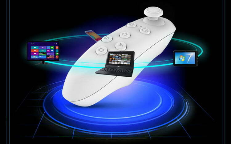
PCB Design of VR Game Controller
VR Gaming Technology Virtual Reality (VR) gaming technology is a rapidly advancing field that enables players to immerse themselves in a computer-generated 3D environment. With advances in hardware and software,
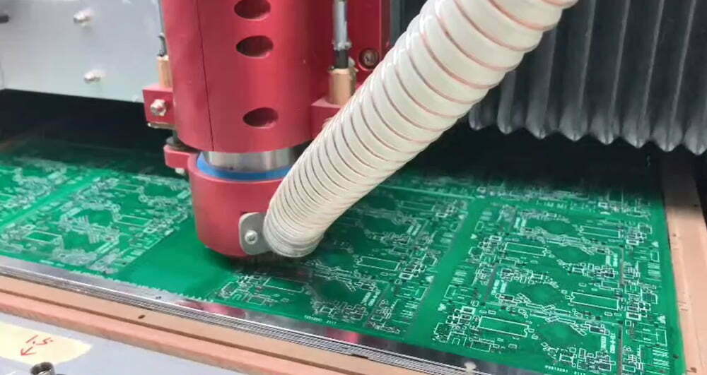
Rapid PCB Prototyping
We have advanced equipment to support rapid PCB prototyping. Depending on the situation, the entire production process takes about one to three weeks. The prototype is first tested in the
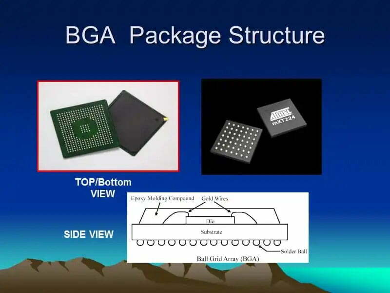
Routing Rules of BGA package in PCB design
BGA is a commonly used component on PCB, usually CPU, NORTH BRIDGE, SOUTH BRIDGE, AGP CHIP, CARD BUS CHIP, etc. They are mostly packaged in bga type. In short, 80%

PCB Design for Capacitance Test Based on Single Chip Microcomputer
This circuit is based on the PCB design of the capacitance test circuit of the PlCl6LF874 microcontroller. The specific contents are as follows. How the Capacitance Measurement Module WorksThe overall

PCB Design of Temperature Control for LED Home Appliances
1. Develop and design cooperation methods:Software design: MCU software development and design, according to customer requirements, write the required functional software; or rewrite the software part according to the customer’s


