In this comprehensive guide, we will explore the various aspects of ENIG, its advantages and disadvantages, applications, and standards, as well as compare it with other surface finishes.
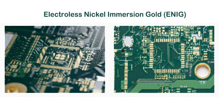
What is ENIG?
Electroless Nickel Immersion Gold (ENIG) is a popular surface finish used in the manufacturing of Printed Circuit Boards (PCBs). This two-layer metallic coating consists of a layer of nickel plated over the copper pads on a PCB, followed by a thin layer of gold.
ENIG Process Overview
The ENIG process includes these steps:
Pretreatment → oil removal → water washing → acid washing → water washing → microetching → water washing → prepreg (H2SO4) → activation (Pd catalyst) → water washing → chemical nickel (Ni/P) → water washing → immersion gold plating → gold recovery → water washing → drying
Pretreatment:
The purpose is to remove the oxides on the copper surface by brushing or sandblasting and to rough up the copper surface to increase the adhesion of subsequent nickel and gold.
Micro-etching:
Sodium persulfate/sulfuric acid to remove the oxide layer on the copper surface and reduce the depth of the gouges caused by brushing during pretreatment. Too deep brush marks often become an accomplice to the attack of the nickel layer by immersion gold.
Activation:
Because the copper surface can not directly start the chemical nickel deposition reaction, so it is necessary to put a layer of palladium (Pd) on the copper surface first to act as a catalyst for the chemical nickel deposition reaction. Using the principle that Cu is more active than Pd, the palladium ion is reduced to palladium metal and attached to the copper surface.
Chemical nickel:
Ni / P, its main role is to block the migration between copper and gold (migration) and diffusion, and as a follow-up to the role of welding and tin chemical reaction to generate IMC elements.
Dip plating gold:
The main purpose of gold in the protection and prevent the nickel layer oxidation, gold in the process of soldering and will not participate in the chemical reaction, too much gold rather than hinder the strength of the solder, so gold as long as enough to cover the nickel layer so that it is not easy to oxidation can be, if you want to make COB (Chip On Board) hit the line on another matter, because the gold layer to have sufficient thickness.
Advantages and Disadvantages of ENIG
ENIG and its variant ENEPIG (Electroless Nickel Electroless Palladium Immersion Gold) were developed as alternatives to more conventional solder coatings, such as Hot Air Solder Leveling (HASL). While these finishes are more expensive and require additional processing steps, they offer several advantages over traditional coatings.
Advantages
- Excellent surface planarity:
ENIG provides a flat surface, which is crucial for mounting components like Ball Grid Arrays (BGAs) and other fine-pitch components. - Good oxidation resistance:
The gold layer protects the nickel from oxidation, ensuring a longer shelf life and improved electrical performance. - High suitability for movable contacts:
Due to its low contact resistance and anti-friction properties, ENIG is ideal for applications like membrane switches and plug-in connectors. - RoHS compliance:
ENIG is an environmentally friendly surface finish that meets RoHS requirements.
Disadvantages
- Higher cost:
ENIG is more expensive than traditional solder coatings like HASL. - Complex processing steps:
The multiple steps involved in the ENIG process can increase the complexity of PCB manufacturing. - Potential for black pad defects:
Early ENIG processes were prone to poor adhesion to copper and the formation of a non-conductive “black pad” layer due to sulfur-containing compounds from the solder mask leaching into the plating bath.
ENIG Standards
The quality and other aspects of ENIG coatings for PCBs are governed by IPC (Institute of Printed Circuits) Standard 4552A, which covers topics like thickness specifications and process control. Additionally, IPC Standard 7095D, which focuses on ball array connectors, addresses some ENIG-related issues and their remediation.
ENIG Thickness Specifications
In an ENIG finish, the nickel layer serves as a barrier to the copper pad, while the gold layer protects the nickel during storage and provides low contact resistance. Typically, the nickel layer has a thickness of 4 to 7 µm, and the gold layer has a thickness of 0.05 to 0.23 µm. These thicknesses are specified by IPC-4552 for ENIG.
Black Pad Defects
One of the primary concerns with ENIG finishes is the potential for black pad defects. Black pad, also known as brittle fracture, is a result of excessive phosphorus that forms during the ENIG process. These defects can lead to weakened metallurgical bonds and eventual failure of the solder joints.
To prevent black pad defects, it is essential to maintain strict control over the nickel bath and carefully monitor the pH level. Improvements in immersion gold technology have also helped reduce the risk of black pad formation by minimizing nickel surface corrosion.
Comparing ENIG with Other Surface Finishes
ENIG is often compared with other surface finishes, such as HASL, OSP (Organic Solderability Preservatives), Immersion Tin, and ENEPIG. Each finish has its advantages and disadvantages, and the choice of surface finish depends on factors like cost, product application, component types, and production volume.
HASL
HASL is a conventional solder coating that offers excellent solderability and low cost. However, it has some drawbacks, including uneven surface planarity and potential compatibility issues with lead-free soldering.
OSP
OSP is an organic-based surface finish that provides a flat surface and good solderability. However, its shelf life is limited, and it may not be as reliable as ENIG in high-density applications.
Immersion Tin
Immersion Tin is a popular surface finish that offers excellent solderability and flatness. However, it has a shorter shelf life than ENIG and is not as resistant to oxidation.
ENEPIG
ENEPIG is an upgraded version of ENIG that adds a thin layer of electroless palladium between the nickel and gold layers. This additional layer helps prevent black pad defects and enhances the finish’s overall performance. However, ENEPIG is generally more expensive than ENIG.
Applications of ENIG
ENIG is widely used in Surface Mount Technology (SMT), lead-free soldering, and BGA packages. It is well-suited for industries such as data/telecom, high-end consumer electronics, aerospace, military, and medical devices. Additionally, ENIG is often preferred in the flex PCB market due to its high reliability and performance.
Conclusion
ENIG is a versatile and reliable surface finish option for PCBs, offering excellent oxidation resistance, surface planarity, and solderability. While it has some drawbacks, such as a higher cost and potential for black pad defects, the benefits it provides make it a popular choice for many PCB applications. By understanding the advantages and limitations of ENIG and comparing it with other surface finishes, PCB designers can make informed decisions when selecting the best surface finish for their projects.