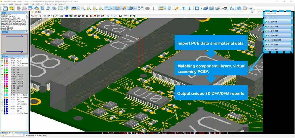
What is DFM?
Design for Manufacturing (DFM) is actually a bridge between R&D and production. It simplifies, optimizes, and improves product design to produce better products at a lower cost.
Why is DFM So Important?
The goal of the enterprise: low cost, high output, good supply capacity, and long-term reliable products. That is to say, better products can be produced with less money, and DFM can meet the needs of enterprises to a large extent. DFM plays a crucial role in ensuring optimal efficiency, rapidity, and utmost productivity.
There is a widespread belief among many individuals that approximately 70% of product manufacturing expenses can be attributed to the initial design phase, encompassing aspects like materials and production. Consequently, DFM possesses a remarkable capacity for cost reduction.
In addition, DFM can also play a role in the entire manufacturing and production process.
Benefits of DFM
- With DFM, production costs can be reduced
- Accelerate time to market
- Reduce development costs
- Minimize the need for revisions or eliminate the need for them altogether
- Reduce rework and rework costs
- Find errors and glitches, and avoid them
- Deliver an elevated level of product excellence by continuously refining and augmenting the design at every stage.
DFM Process Requirements for PCB Design
PCB Size
Dimensions shall not exceed the processing capacity of the equipment. At present, the commonly used size range is “width (200 mm ~ 250 mm) x length (250 mm ~ 350 mm)”. For PCBs with a long side size less than 125mm or a short side smaller than 100mm, or irregular irregular shapes around the PCB, it needs to be designed as a puzzle.
PCB Shape
The shape of the board is rectangular. If you do not need to join the board, the 4 corners of the board are required to be rounded; if you need to join the board, the 4 corners of the board after the board are required to be rounded, and the minimum radius of the rounded corner is r=1mm. The recommended value is r=2.0mm.
In order to ensure the stability of the transmission process, the design should consider the use of process jigsaw to convert the irregularly shaped PCB into a rectangular shape, especially the corner gaps should be filled.
For pure SMT boards, gaps are allowed, but the size of the gap must be less than 1/3 of the length of the side to ensure that the PCB is conveyed smoothly on the chain.
 1")
For fillets, a minimum radius of 0.8mm is recommended, and radii as small as 0.4mm can be used if required.
The design requirements for the golden fingers are shown in the figure, except that the chamfering of the insertion side is designed according to the requirements, the two sides of the plug-in board
A chamfer of (1~1.5)×45° or a rounded corner of R1~R1.5 should also be designed.
 2")
Transmission Side
To minimize PCB deformation during soldering, it is customary to employ the longer side as the transmission direction for PCBs that don’t require imposition. Similarly, when imposition is necessary, the longer side direction should also be utilized as the transmission direction. For PCBs with a ratio of short side to long side greater than 80%, the short side can be used for delivery.
Since the terminal board generally adopts a jigsaw design, the process side is generally used as the transmission side, and the narrowest width of the process side is generally not less than 4.5mm.
MARK Points
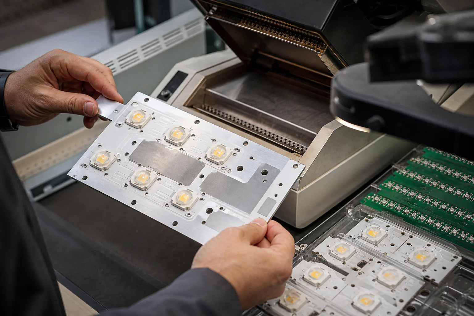
Optical positioning fiducial marks, also known as MARK points, play a crucial role in the assembly process. These mark points, often referred to as reference points, serve as consistent and measurable indicators, facilitating precise alignment of circuit patterns throughout all assembly steps. Their primary function is to ensure accurate positioning of each component. Consequently, mark points hold immense significance in SMT production.
During circuit board design, the Mark point acts as a positional identifier for affixing the PCB onto the automatic placement machine. The selection of mark points directly affects the efficiency of component placement performed by the automatic placement machine.
Mark Point Types:
Generally, the selection of Mark points is related to the model of the automatic placement machine. There’re 3 kinds of options:
- Single Board Mark:
All products produced by SMT must have at least one pair of MARK points within each PCB that meet the design requirements for identification by SMT machines, such as single board mark. - Piecing Board Mark:
The piecing board mark only plays a role in assisting positioning. The special way of piecing board are:
1) The diagonal mark position must be the same for the yin and yang board.
2) Mirror board mark position must be the same. (R1=R2) Local Fiducial Mark:
Local Fiducial Mark is used for positioning individual components such as QFP and BGA, it can improves placement accuracy.
 3")
Mark Point Shape:
The preferred shape of the mark point is a solid circle with a diameter of 1mm (±0.2mm), and the material is bare copper (which can be protected by a clear anti-oxidation coating), tin-plated or nickel-plated, and attention should be paid to the flatness and edge Smooth and neat, the color is clearly different from the surrounding background color. In order to ensure the recognition effect of printing equipment and SMT equipment, there should be no other wiring, silk screen, pad or Wait-Cut in the open area of MARK point.
Mark Point Size:
1) The minimum diameter of the Mark point is 1.0mm, and the maximum diameter is 3.0mm. Mark punctuation: Note that the dimensional change on the same printed board cannot exceed 25 microns;
2) Of particular significance is the uniformity in size of all Mark points across PCBs bearing the same board number. This requirement applies to all PCBs, including those with identical plate numbers manufactured by the same company.
3) It is recommended that RD-layout unify the Mark point marking diameter of all image files to 1.0mm;
Mark Point Edge Distance:
1) The Mark point (edge) must be ≥5.0mm from the edge of the printed board (the minimum spacing between the machine clamp PCB Requirements), and must be in the PCB board instead of the board edge, and meet the minimum mark point openness requirements. Emphasis: It refers to the distance between the edge of the MARK point and the edge of the board ≥ 3.0mm, not the center of the MARK point.
Mark Point Edge Radius:
In the vicinity of the Mark point, it is crucial to maintain an unoccupied zone devoid of additional circuitry elements or markings. The radius of the clear circular area surrounding the Mark point should be equal to or greater than twice the radius (2R) of the Mark point itself. For improved machine recognition, a radius (r) of three times the Mark point radius (3R) is preferred. It is also advisable to enhance the color contrast between the Mark point and its surrounding environment. No characters are allowed in r (copper or silk screen, etc.) Regarding the material selection for Mark points, several options are available. Mark points can be composed of bare copper, bare copper shielded by a transparent anti-oxidation coating, nickel or tin-plated, or coated with solder. If solder mask is used, it should not cover the Mark point or its open area.
MARK Points Positioning:
To ensure precise component placement, the Mark points on the circuit board or composite board should be positioned diagonally as far apart as possible, preferably distributed along the longest diagonal.
Mark Point Flatness:
The surface flatness tolerance for Mark point markings should fall within the range of 15 microns [0.0006′], ensuring a level and even surface.
Positioning Holes:
Each PCB should be designed with at least two positioning holes at its corners. In a jigsaw panel, there should be four positioning holes distributed in the four corners. The standard aperture of the positioning holes is 2.00±0.08mm, and the distance between the center of the positioning hole and the board’s edge should be 5mm. Components or pads adjacent to the alignment hole should have a minimum distance of 1.5mm from the edge of the alignment hole.
MARK Points Validity:
The validity of MARK points is dependent on their appearance in pairs along the same diagonal. To optimize performance, it is crucial to ensure a noticeable contrast in visual appearance between the Mark point mark and the substrate material of the printed board. Additionally, consistency in the inner background of all Mark points is essential, requiring them to remain identical.
Avoid Hole Metallization:
Positioning holes and non-grounding mounting holes are generally designed as non-metallized holes to avoid any metallization issues.
How to Apply DFM in Product Production?
Start with the Schematic Diagram
In the process of schematic diagram design, the designer’s material selection revolves around fulfilling the intended functionality. However, it is essential to consider an array of supplementary factors, encompassing price, reliability, and the material’s life cycle, to make informed choices. If you start thinking about it at the design stage, you can save a lot of trouble, and you can avoid the trouble of the manufacturer.
Here I have to talk about BOM. There are many matching material selections on the market, which can actually solve a lot of problems.
PCB Layout
The PCB layout holds significant importance within the overall design process. During the initial design phases, pivotal decisions regarding the board’s configuration directly impact its manufacturing process.
1) Single-layer board, double-layer board or multi-layer board
Two-layer boards are often used for signal integrity and thermal management, while also considering the manufacturability of the board. For example, determining the board thickness required for the vias used is the optimum drill aspect ratio, which requires using a different board material or changing the number of layers of the board.
2) Board model outline
Determine the model and outline of the PCB, requiring detailed circuit board shape and size, including placing fixed components, through holes, slots, etc. Care must be taken here so that redesign and assembly errors can be avoided. (Vigilance is crucial in this aspect to mitigate the risks of redesigning and assembly errors.)
3) Materials
In order to avoid soldering problems during assembly, it is necessary to have the materials ready.
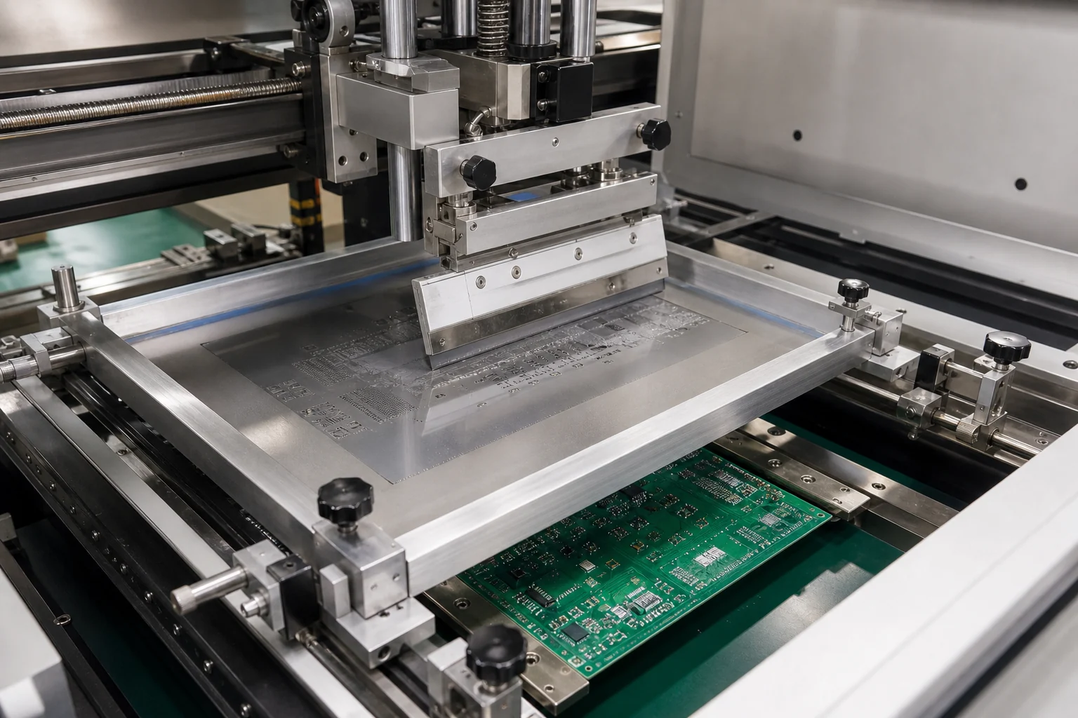
Place and Route According to DFM Requirements
When it comes to PCB component placement and routing, achieving the shortest signal paths is paramount, particularly in high-speed and power circuits, to optimize electrical performance. During the board layout process, it becomes imperative for the PCB designer to strike a harmonious equilibrium between the electrical requirements and the manufacturing constraints of the board.
SMD
In order for the mounting machine to automatically mount, it is definitely necessary to keep a certain distance between components, and of course there are some that cannot avoid manual soldering.
- plug-in and patch need to be placed perpendicular to the board through the direction of the solder wave, which facilitates the uniform distribution of solder around the component pins.
- the placement of the plug-in will also affect the solder, for example, when the plug-in and patch are on the same side of the PCB board, reflow soldering will be before the wave soldering to carry out.
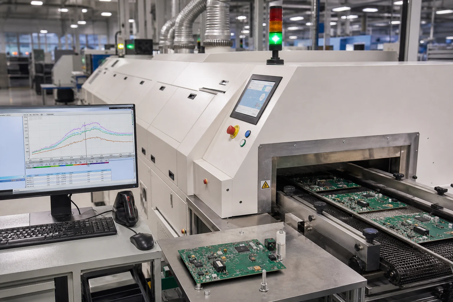
Reflow soldering
- Smaller discrete SMT parts with two pins need to be thermally balanced for reflow soldering.
- When a pad is connected to a large area of metal, it can act as a heat sink and cause the solder paste on that pad to reflow more slowly than the other pad, resulting in a standing part monument.
- Pad size is also an issue, as pads that are too large may cause the part to float out of alignment, while pads that are too small may not hold enough solder paste to reflow into a solid connection.
PCB packages
- Too large through-holes for their pins may disperse solder through them too quickly, resulting in poor solder connections.
- Too large SMT pads may contain too much solder paste, which may bridge to adjacent pads and lead to short circuits.
- Too close to the pads are also prone to solder bridging. This is often seen in fine pitch components where there is not enough solder barrier between the pads to prevent this.
Design Finalization and Documentation
Beyond the aspects of component placement and routing, there exist numerous other responsibilities entailed within the PCB layout phase that profoundly impact the manufacturability of the board.
PCB Testing
To verify the accuracy of the assembly process, boards often include test points that are accessible to the test fixture’s probes. However, if test points are not included in the original design, the board must be redesigned to add them before it can go into production. Redesigns like this are not only costly and time-consuming, but can also introduce new DFM issues that did not previously exist.
Silkscreen and Board Marking
Silkscreen markings are important for PCB testing, rework, and debugging. Without the necessary information on the board, manufacturing can be slowed while rework and test technicians look for specific part or polarity markings.
Design Summary Drawings
Without complete and accurate design modification information, time can be wasted in verifying manufacturing details. Time, or even worse, errors, can occur during the production of the board.