Introduction to NOR Flash and NAND Flash
NOR Flash
Intel first developed the Nor Flash technology in 1988. Nor Flash is characterized by on-chip execution (XIP, eXecute In Place), and its reading is similar to the random reading form of our common SDRAM. Users can directly run the program loaded on the Nor Flash The code inside, which can reduce the capacity of SRAM and save cost. Because of its fast reading speed and less error-prone, it is mostly used to store important information such as programs and operating systems.
NAND Flash

In 1989, Toshiba Corporation published the Nand Flash structure, emphasizing lower cost per bit, higher performance, and it can be easily upgraded through the interface like a disk. Nand Flash does not adopt the random read technology of memory. It reads in the form of reading one block at a time, usually 512 bytes at a time. The implementation of memory provides a cheap and effective solution.
Nand flash memory has the advantages of large capacity and fast rewriting speed, and is suitable for storing large amounts of data, so it is more and more widely used, such as embedded products including mobile phones, digital cameras, and U disks.
NOR Flash Vs. NAND Flash
NOR and NAND are the two main non-volatile flash memory technologies on the market. Intel first developed NOR flash technology in 1988, which completely changed the situation where the market was monopolized by EPROM and EEPROM. Then, in 1989, Toshiba released the NAND flash structure, emphasizing the reduction of cost per bit, higher performance, and it can be easily upgraded through the interface like a disk. Here we explain the difference between them:
| Feature | NAND Flash | NOR Flash |
|---|---|---|
| Capacity | Large | Small |
| Access Mode | Sequential Read/Write | Random Read/Write |
| Interface | Any I/O | Specific Full Memory Interface |
| XIP (Executable Code) | Not Supported | Supported |
| Read/Write Performance | Block Read (Sequential), Block Write, Block Erase (Erase by Block) | Block Read (RAM Mode), Slow Write, Slow Erase |
| Endurance | Approximately One Million Times | Approximately One Hundred Thousand Times |
| Price | Low | High |
| Applications | USB Drives, Memory Cards, SSDs, and Embedded Storage (eMMC, eMCP, UFS) | Automotive Electronics and IoT, 5G and Smartphones, and Accessories (such as TWS Earphones and Wearable Devices) |
Performance Comparison
Flash memory is non-volatile memory that can be erased, written and reprogrammed in blocks of memory cells called blocks. The write operation of any flash device can only be performed in empty or erased cells, so in most cases, the erase must be performed before the write operation.
It is very simple for NAND devices to perform erasing operations, while NOR requires that all bits in the target block be written to 0 before erasing. Since erasing NOR devices is performed in blocks of 64-128KB, the time to perform a write/erase operation is 5s. On the contrary, erasing NAND devices is performed in blocks of 8-32KB. The operation takes only 4ms at most. The difference in block size when performing erase further widens the performance gap between NOR and NAND, statistics show that for a given set of write operations (especially when updating small files), more erase operations must be performed in carried out in NOR-based units. Thus, designers must weigh the following factors when selecting a storage solution.
- The reading speed of NOR is slightly faster than that of NAND.
- The writing speed of NAND is much faster than that of NOR.
- NAND’s 4ms erasing speed is much faster than NOR’s 5s.
- Most write operations require an erase operation first.
- The erasing unit of NAND is smaller, and the corresponding erasing circuit is less.
In addition, the actual application of NAND is much more complicated than that of NOR. NOR can be used directly and code can be run directly on it; while NAND requires an I/O interface, so a driver is required for use. However, today’s popular operating systems support NAND-structured Flash. In addition, the Linux kernel also provides support for NAND-structured Flash.
Interface Comparison
NAND devices use complex I/O ports to access data serially, and the methods of each product or manufacturer may vary. 8 pins are used to transmit control, address and data information.
NOR Flash has an SRAM interface, has enough address pins to address, and can easily access every byte inside it.
Capacity and Cost Comparison
NAND Flash is mainly used in 8-128MB products, suitable for data storage, and its unit size is almost half that of NOR devices, and the structure can also provide higher capacity within a given mold size, thereby reducing the cost accordingly. Price: NOR Flash occupies most of the flash memory market with a capacity of 1-16MB, and is mainly used in code storage media, and its price will be higher than that of NAND.
Reliability and Durability Comparison
1. Durability (life)
In NAND flash memory, the maximum number of erasing and writing of each block is one million times, while that of NOR is 100,000 times.
2. Bit swapping
All Flash devices suffer from bit swapping: under certain conditions, a bit is inverted or reported as inverted. If it happens to a critical file, it can cause serious system downtime. After a bit change, a bit is inverted or reported as inverted. This problem is more common in NAND flash memory. NAND suppliers recommend using EDC/ECC algorithms when using NAND flash memory.
3. Bad block processing
Bad blocks in NAND devices are randomly distributed. NAND devices require an initial scan of the media to find bad blocks and mark the bad blocks as unusable. In fabricated devices, failure to perform this process by reliable methods results in high failure rates.
Use Comparison
The use of NAND Flash is more complicated, and the driver must be written before continuing to perform other operations. Writing information to the NAND device also requires certain skills, and virtual mapping must be performed from beginning to end.
The use of NOR Flash is relatively simple, you can directly use NOR-based flash memory, you can connect it like other memories, and you can run code directly on it.
Software Support Comparison
When running code on NAND devices, a driver, also known as a memory technology driver (MTD), is usually required, but no software support is required when using NOR devices. Both require MTD for write and erase operations.
How Does NOR and NAND Flash Work?
Method of Storing Data
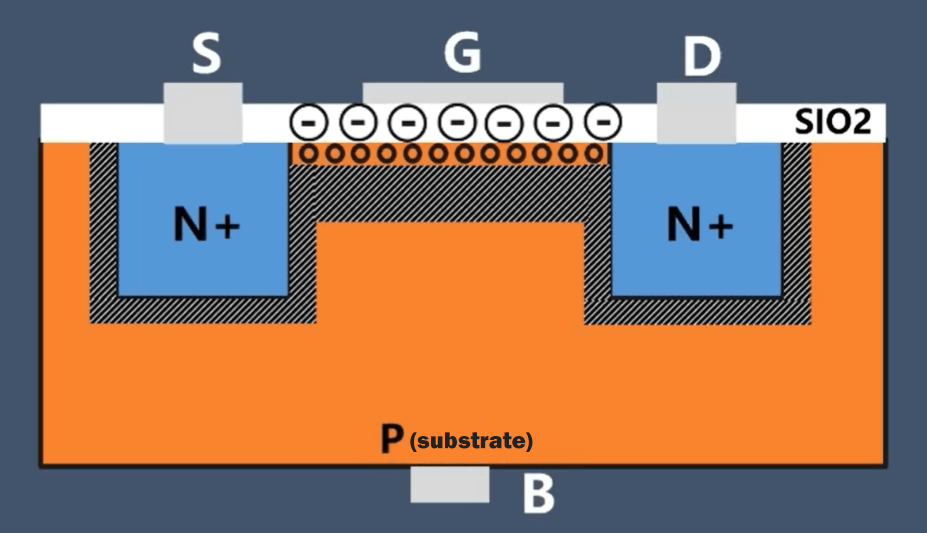
Both NOR and NAND flash memories use three-terminal devices as storage units, which are source, drain and gate. The working principle is the same as that of field effect transistors, mainly using the effect of electric field to control the source and drain. The current consumption of the gate is extremely small. The difference is that the field effect transistor has a single gate structure, while Flash has a double gate structure, and a floating gate is added between the gate and the silicon substrate. . The floating gate is made of nitride sandwiched between two layers of silicon dioxide material. The nitride in the middle is the charge potential well that can store charge. The thickness of the upper and lower oxide layers is greater than 50 angstroms to avoid breakdown.
Redischarge of the Floating Gate
The process of writing data into the data cell is the process of injecting charge into the charge potential well. There are two techniques for writing data, hot electron injection and F-N tunneling (Fowler Nordheim tunneling). The former is to feed the floating gate through the source Charging, the latter is to charge the floating gate through the silicon base layer. NOR-type Flash charges the floating gate through hot electron injection, while NAND charges the floating gate through the F-N tunneling effect. Before writing new data, the original data must be erased first. This is different from the hard disk, that is, the charge on the floating gate is released. Both types of Flash are discharged through the F-N tunneling effect.
Connection and Addressing Mode
The two kinds of Flash have the same storage unit, and the working principle is the same. In order to shorten the access time, it is not a separate access operation for each unit, but a collective operation for a certain number of access units.
The storage units of NAND-type Flash are connected in series, while the units of NOR-type FLASH are connected in parallel; in order to effectively manage all storage units, the storage units must be uniformly addressed. NAND devices use multiplexed I/O ports to access data, and 8 pins are used to transmit control, address and data information in time-sharing. All storage units of NAND are divided into several blocks, and each block is divided into several pages, each page is 512byte, that is, 512 8-digit numbers, that is to say, each page has 512 bit lines, each bit line There are 8 storage units; so each time NAND reads data, it specifies the block address, page address, and column address (the column address is the starting address in the read page).
Each storage unit of NOR is connected to the bit line in parallel, it has an SRAM interface, there are enough address pins to address, and it is easy to access every byte inside it. It is convenient for random access to each bit, and it does not need a driver; it has a dedicated address line, which can realize one-time direct addressing; it shortens the execution time of Flash to processor instructions.
Application of NOR and NAND Flash
NOR Flash
The NOR flash is primarily utilized for storing and executing code and data in devices such as microcontrollers, embedded systems, digital cameras, smartphones, and solid-state drives (SSDs).
NAND Flash
The application of NAND flash in solid-state storage can be extended to military, vehicle, industrial control, video surveillance, network monitoring, network terminals, electric power, medical, aviation, navigation equipment and other fields.
Therefore, NOR flash is more suitable for occasions of frequent random reading and writing. It is usually used to store program codes and run directly in flash memory. Mobile phones are big users who use NOR flash memory; NAND flash is mainly used to store data. Our commonly used flash memory products, such as Flash drives and digital memory cards all use NAND flash memory.