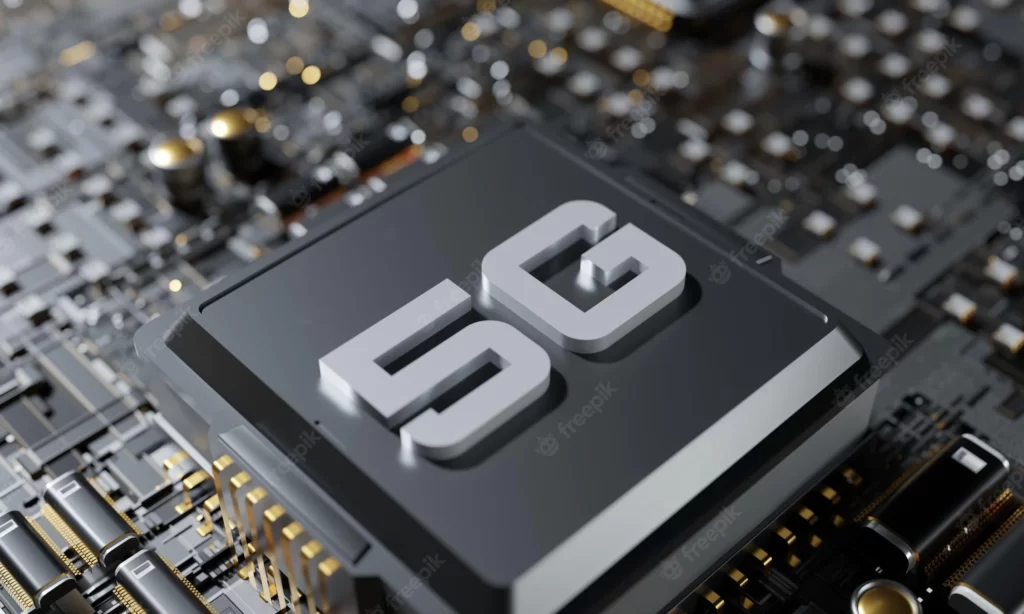
The adoption and implementation of 5G connectivity are underway, as mobile carriers race to be the first company with a 5G network. A key enabler of 5G is low latency, high bandwidth, and high cell density. These three capabilities require operators to adopt new technologies that support denser antennas and millimeter wave frequencies in their networks. Those new technologies are what’s called “5G-ready” or “5G-capable.” This article will explore what makes a PCB a 5G PCB, the various methods for designing a 5G PCB, the implications for manufacturers of these boards, and how you can prepare for the advent of 5G PCB manufacturing.
What is 5G Technology?
5G technology is the key enabler for a wide range of exciting new products and industries that are just starting to take shape. From autonomous vehicles to the Internet of Things, to ultra-low latency networks for finance, healthcare, and other critical infrastructure, there’s a lot of promise and opportunity.
First, 5G is not a product. It’s not a single technology or product that you can put on a shelf and then plug in to get the results you want. Rather, 5G is an overall concept that refers to an upgrade in the mobile telecommunications standard that powers the world’s wireless networks. The reason for the upgrade is simple: wireless networks are getting more and more crowded. Every year, more and more people are getting smartphones and using mobile data to access the internet. That’s leading to more customers for wireless carriers, but also more demand on their networks.
5G Communication Protocols
One of the key factors that will affect the implementation of 5G is the communication protocol. 5G will rely on a handful of communication protocols – New Radio (NR) being one of them. NR is the 5G standard that will allow for the low latency, high bandwidth, and high cell density that are required for 5G.
Other key communication protocols include:
– SC-FDMA (single-carrier frequency-division multiple access)
– OFDM (orthogonal frequency-division multiplexing)
– MIMO (multiple-input, multiple-output)
These communication protocols make use of higher frequencies that allow for lower latency, and higher bandwidth, and a higher cell density. They also make use of Beamforming to focus the signals. This is a critical feature for indoor coverage in both commercial buildings and homes.
Why is 5G Manufacturing Important?
Manufacturers of critical components like PCBs will have to adapt their operations to support the higher frequencies used for 5G. Those frequencies are well outside the range used for 4G and even LTE networks. For example, typical LTE antennas operate in the 700 MHz range. The initial standards for 5G have specified frequencies in the 28 GHz and 39 GHz range. That’s an increase of almost four times the frequency. To make matters worse, the 5G antennas will be much smaller than the typical LTE antennas. That means they will be less efficient and use more board real estate. And that means the components that go on the boards will have to be smaller too.
Implications of 5G PCB Manufacturing
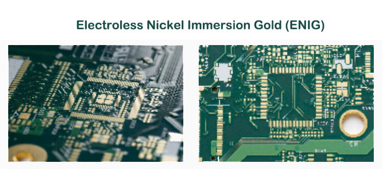
One of the implications of 5G PCB manufacturing is that it will require manufacturers to transition to shorter trace lengths and smaller printed circuit board (PCB) trace widths. All of this is to support the higher frequencies and smaller antennas. To make matters worse, the smaller antennas will allow less tolerance in the PCB board fabrication process.
That means smaller variations from board to board. But the transition to lower frequencies will have several implications for PCB manufacturers. They will have to change their existing equipment to process the higher frequencies. More importantly, the existing equipment might not be able to make the transition. It’s almost certain that some of the existing equipment will not be able to make the transition to support 5G PCB manufacturing.
How to Design a 5G PCB?
The first step in designing a 5G PCB is to understand the operating frequency and how it will affect the board layout. Then you can select the appropriate board design rules. For example, if you’re making a board for the 28 GHz frequencies, you’ll want to use the millimeter wave board design rule parameters to get a design that works.
The next step is to select the transmission line types. 5G will require wider traces to support the higher frequencies. And wide traces are more susceptible to EMI. So you’ll want to use lower-impedance transmission lines like microstrip. Finally, you’ll want to make sure that you select materials that have the appropriate impedance and thickness. For example, 6 mil copper will be the best choice for most 5G boards.
Millimeter Wave PCB Design Rule Basics
There are a few basic design rules to keep in mind when designing a printed circuit board (PCB) for a millimeter wave (mmWave) system.
- First, the trace widths and spacing between traces must be much smaller than what is typically used for lower frequency systems. This is necessary to prevent signal attenuation and reflections.
- Second, the dielectric constant of the PCB material must be as low as possible to minimize signal loss.
- Finally, the PCB should be designed with as few layers as possible to reduce the risk of signal crosstalk.
5G PCB Manufacturing Challenges
There are several challenges in designing and manufacturing 5G PCBs. One of the challenges is that most standard design tools don’t support 5G frequencies. 5G is a brand new standard. So designers and engineers operating at 28 GHz and above are literally designing a new technology. And that means there won’t be many standard design tools available for designing a 5G PCB.
Engineers will have to use a combination of computer-aided design (CAD) tools, simulation tools, and other design tools. Another challenge will be the high level of noise at the higher frequencies. That means designers will have to use low-impedance transmission lines like microstrip. But designers will also have to be careful about plated through holes and other high-density components.