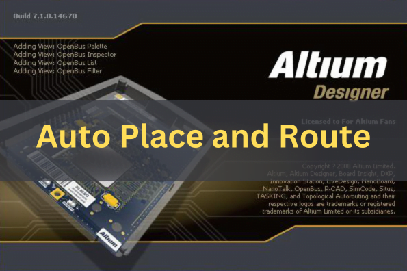
When designing a PCB, in order to improve efficiency, we need to learn how to automatically place and route our projects. In this tutorial, we will introduce the auto place and route in Altium Designer.
Auto Placing Components
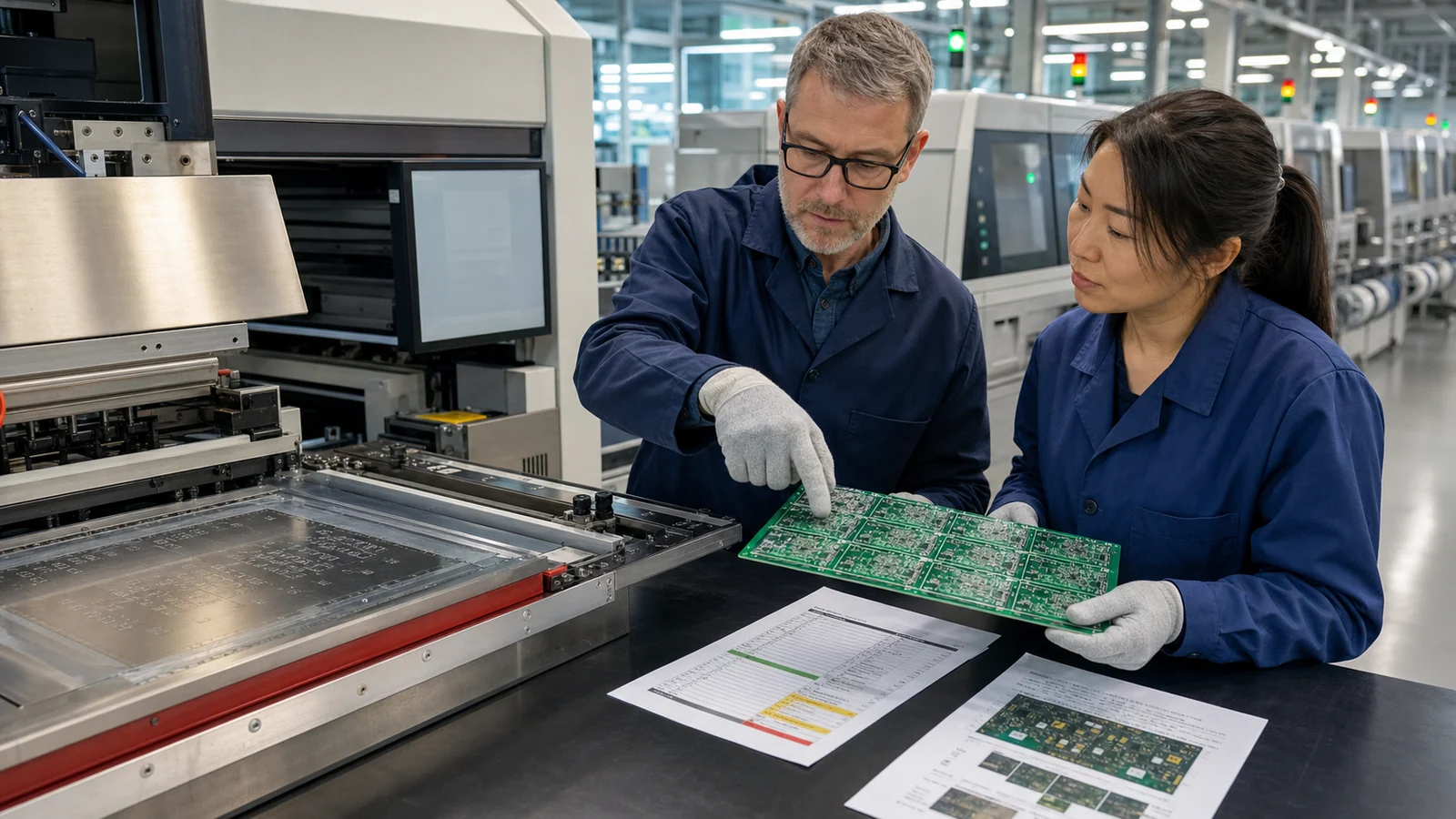
1. Select the components to be placed automatically in the PCB, generally according to the circuit module.

2. Select Tools-Component Placement-Reposition Selected Components in the menu bar.

3. Place the components according to the circuit requirements, and click the left button to complete.

Auto Routing
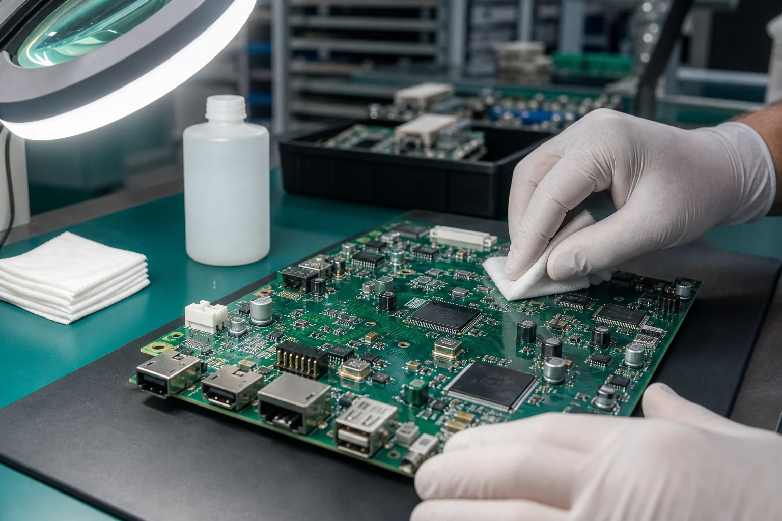
First, open the Altium Designer software, then open your own PCB file.

The figure below is an example of a PCB file that has been laid out, and now we want to automatically route it.

Select Auto Route – ALL. Route the entire PCB diagram.

In the pop-up dialog box, here you can edit layer directions and rules, select routing strategy, and then click “Route All” in the lower right corner to perform automatic routing.

The figure below is the process of routing and the result after completion.


The final step is to manually modify the routing. Although the auto routing is efficient, there may be deviations in the thickness and direction of some lines, which we need to check and correct manually.

Engineering checks for Altium auto place and route review for manufacturable PCBs
Before using Altium auto place and route review for manufacturable PCBs in a PCB, firmware, repair, or validation workflow, confirm the details that usually decide whether the design works reliably instead of only reading the headline specification.
Design and troubleshooting checklist
| Area | What to check | Why it matters |
|---|---|---|
| Constraint setup | Define clearance, width, differential pairs, classes, keepouts, and rooms before autorouting | Autorouters follow constraints; weak rules produce weak layouts |
| Placement quality | Lock connectors, power parts, crystals, decoupling capacitors, and thermal components first | Critical placement decisions should not be delegated to automation |
| Post-route checks | Run DRC, return-path review, length tuning, copper balance, and assembly clearance checks | A routed board still needs engineering review before fabrication |
These checks help connect the search intent around Altium auto placement with practical board-level decisions, component selection, and failure analysis.