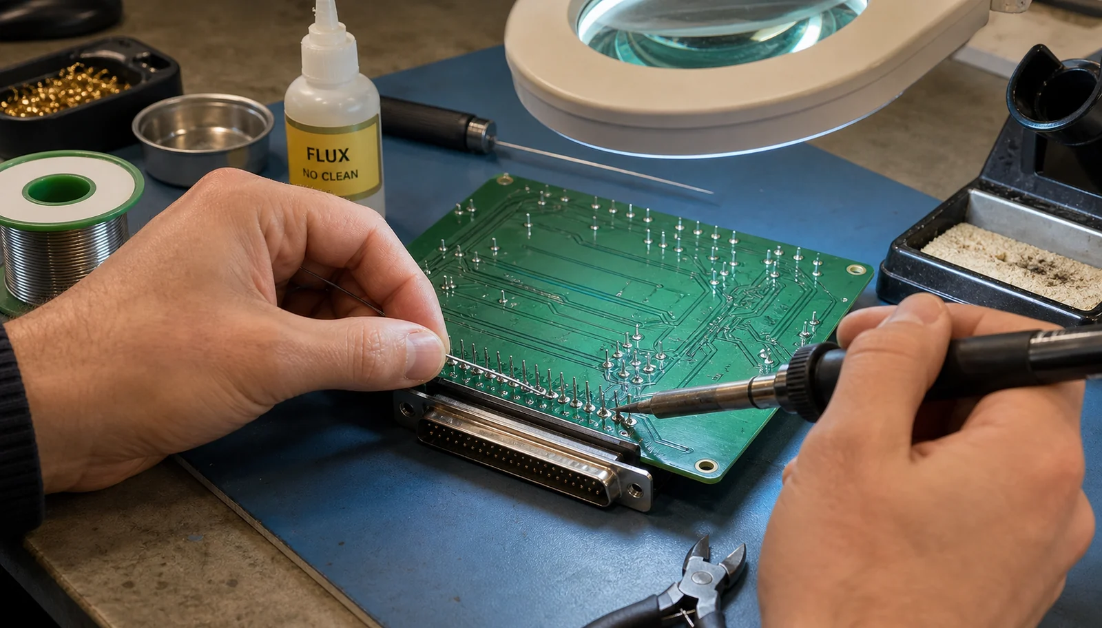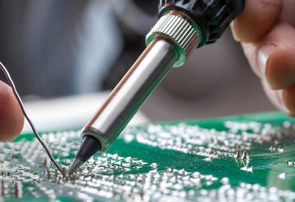
Wicking solder is a common issue encountered in the electronic industry. It occurs when the solder flows away from the intended pad on a Printed Circuit Board (PCB) and accumulates on the surface, entering nearby via holes and tracks. This article will provide an in-depth understanding of wicking solder, its causes, effects, and potential solutions.
Understanding Wicking Solder
Wicking solder, also known as solder drainage or solder escape, occurs when the solder moves away from the intended pad on a PCB and accumulates in undesired locations. The component terminal typically has a lower melting point than the pad to which it is being soldered. As a result, the component terminal reaches its melting point before the pad, causing the solder to flow away and accumulate in unwanted areas.
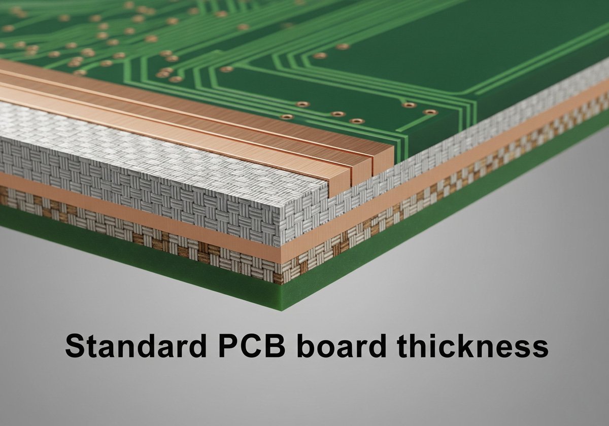
Factors such as the temperature difference between the pad and terminal, wettability of the pad, gap dimensions between pad and lead, and the melting time of solder at the rivet can all contribute to wicking solder problems.
Causes of Wicking Solder
There are several primary causes of wicking solder, which include:
- Low melting points of component terminals:
The component terminal typically has a lower melting point than the pad, causing the solder to flow away from the pad and accumulate in undesired areas. - Varying reflow profiles:
The reflow profile of the solder material can also contribute to wicking solder. This depends upon the amount of tin and lead (Pb) used while preparing the solder alloy. - Unprotected vias and copper tracks:
Vias and copper tracks are not protected by the solder mask layer, making them more susceptible to wicking solder issues. - Inadequate soldering techniques:
Poor soldering techniques can lead to uneven heat distribution and improper solder flow, resulting in wicking solder.
Effects of Wicking Solder on PCBs
When wicking solder occurs, it can cause several negative effects on PCBs, such as:
- Weak solder joints:
The soldering process is crucial for creating strong connections between components and PCB pads. Wicking solder can result in weak solder joints, decreasing the overall reliability of the PCB. - Bridging:
Bridging occurs when solder flows between two adjacent pads, creating an unintended electrical connection. This can lead to short circuits and other issues in the electronic circuit. - Bumps on the backside of the board:
In extreme situations, wicking solder can reach the backside of the board through vias, forming bumps on top of them. These bumps can cause interference with other components and disrupt the functionality of the PCB.
Methods to Evaluate Wicking
It is essential to measure and evaluate wicking solder to ensure the quality and reliability of PCBs. The process typically involves examining processed holes and measuring the extent of wicking after plating the test panel. Cross-sections performed at a 90-degree angle can help confirm the presence of wicking.
Failure to measure wicking solder accurately can lead to faulty results. Accurate measurements must consider the starting and stopping points of the wicking. Adhering to industry standards and norms for production specifications is crucial to maintain modern production processes in line with current demands.
Preventing Wicking Solder
To control and prevent wicking solder, several factors must be addressed:
- Temperature difference between pad and terminal:
Ensuring the pad and terminal reach their melting points simultaneously can help prevent wicking solder. Adjusting the soldering temperature and technique can help achieve this balance. - Wettability of pad:
Improving the wettability of the pad (its joining capability) can help reduce wicking solder problems. This can be done by using appropriate solder alloys and maintaining clean surfaces for soldering. - Gap dimensions between pad and lead:
Adjusting the gap dimensions between the pad and lead can help control the flow of solder and reduce the risk of wicking solder. - Melting time of solder:
Controlling the melting time of solder at the rivet can help prevent wicking solder. This can be achieved by adjusting the soldering temperature and technique.
How Can We Help you with Wicking Solder Issues?
When dealing with wicking solder issues, it’s essential to seek professional assistance to ensure the quality and reliability of your PCBs. Our expert guidance can help you address wicking solder problems and provide solutions tailored to your specific needs.