What is 6-Layer PCB Manufacturing?
6-layer PCB manufacturing is the mass-production of PCBs with a minimum of six layers. In a 6-layer PCB, the top and bottom layers are usually made of laminated material which is then covered with a dielectric layer, enameling, and a conductive layer. The most common manufacturing process of PCB in 6-layer is the film-cut-route (FCR) and film-route-cut-route (FRCD) processes. In other words, these manufacturing processes are used to create a 6-layer PCB on the base of a copper film and then cut the copper film into individual boards for different products. The advantages of the 6-layer manufacturing are ease of manufacturing and low cost.
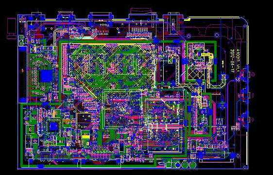
Structure of 6 Layer PCBs
The layers in a 6-layer board are as follows: – Board substrate – Substrate coating – Conductive layer – Enamel – Substrate coating – Board substrate The board substrate is the base material of the board, which is usually an FR-0 or FR-1 material. The substrate coating is a thin layer on the substrate, usually made of polyimide or polyamide. The substrate coating is usually a dissolved polyester. The substrate coating is usually a thickness of 0.33 to 0.35 mm. The conductive layer is a layer of copper, aluminum, or aluminum-tungsten. The conductive layer is the final layer on the board, and it makes the board conductive. The enamel layer is a layer of gold, silver, or copper. The enamel layer is a layer on the conductive layer, which makes the board suitable for use. The substrate coating, conductive layer, and enamel layer are all dissolved in a solvent and then coated onto the board substrate.

Applications of the 6-Layer PCB
– Modular Interconnect Systems
– Modular and Semiconductor Systems
– Semiconductor Devices
– Connectors and FPCs
– Telecommunications and Control Systems
– Consumer Electronics
– Medical Electronics
– Automotive Electronics
– Industrial Control Systems
– Aerospace Systems
– Military Systems
– Oil and Gas Systems
Why Choose 6-Layer PCB Manufacturing?
One of the most important aspects of 6-layer PCB manufacturing is that it allows for large-scale production. The standard for 6-layer manufacturing is for mass production. This mass production helps cut down on the production time and allows for the manufacturer to have a reliable supply of materials. Mass production allows for the manufacturer to meet a large demand for the 6-layer PCBs, which can help manufacturers meet the high demand for these types of boards. While 6-layer PCB manufacturing can meet the demand for functional boards, it cannot meet the demand for reliability. High-reliability boards require a PCB that has more than 6 layers. The extra layers provide the PCB with more strength and ductility.
types of stack-up
The following is the typical 6-layer PCB circuit board stacks for reference. For the combination of six-layer boards, we recommend the scheme 3 first. The priority wiring layers are S2 (stripline), S3, and S1.

Type 1
Top (signal layer)
L2 (ground plane)
L3 (signal layer)
L4 (signal layer)
L5 (power plane)
bottom (signal layer)

Type 2
Top (signal layer)
L2 (signal layer)
L3 (ground plane)
L4 (power plane)
L5 (signal layer)
Bottom (signal layer)
Compared with scheme 1, scheme 2 ensures that the power supply and ground planes are adjacent to reduce the power supply impedance, but S1, S2, S3, and S4 are all exposed, and only S2 has a better reference plane.

Type 3
Top (signal layer)
L2 (ground plane)
L3 (signal layer)
L4 (power plane)
L5 (ground plane)
Bottom (signal layer)
The scheme 3 reduces one signal layer and adds an internal electrical layer. Although the layers available for wiring are reduced, this scheme solves the common defects of scheme 1 and scheme 2.

Type 4
Top (signal layer)
L2 (ground plane)
L3 (signal layer)
L4 (ground plane)
L5 (power plane)
Bottom (signal layer)
For a small number of local signals, the requirements are higher. Option 4 is more suitable than option 3, it can provide an excellent wiring layer S2.

Type 5
Top (signal layer)
L2 (ground plane)
L3 (signal layer)
L4 (power plane)
L5 (signal layer)
Bottom (signal layer)
PCB Manufacturing Process
The manufacturing process of 6 layer pcb involves creating a multilayered circuit board by stacking sheets of copper foil, each with a different electrical property. The layers are then bonded together and etched with a chemical to create an electrical circuit. The process is similar to that of single-sided boards, but the additional layers require a different etching process. A 6-layer board is essentially two 3-layer boards bonded together, so the manufacturing process is the same as for a 3-layer board, with an extra etching step at the end where all the copper layers are etched together. Below are the full steps for reference:
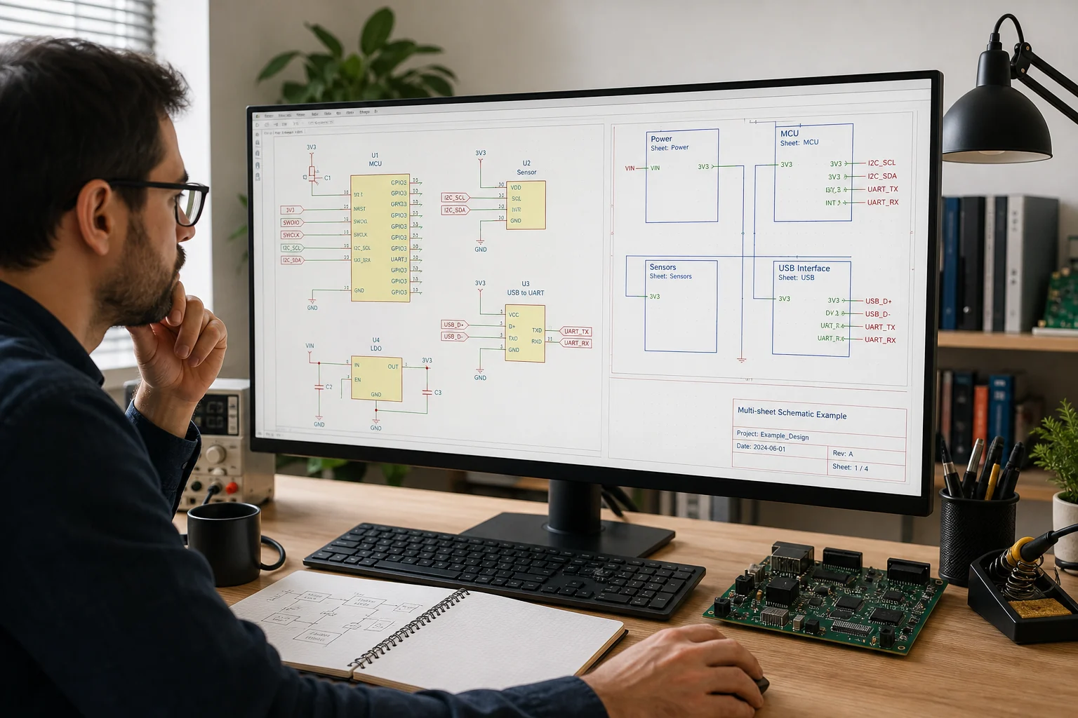
Step 1: PCB Schematic Design and Layout
The first step in the PCB manufacturing process is to design the circuit board. This involves creating a schematic diagram on a computer using special design software. The design should consider the desired purpose of the board, the components that are needed, and any special requirements such as size and shape. Once the schematic has been created, the design is laid out on the board and the exact placement of components is determined.
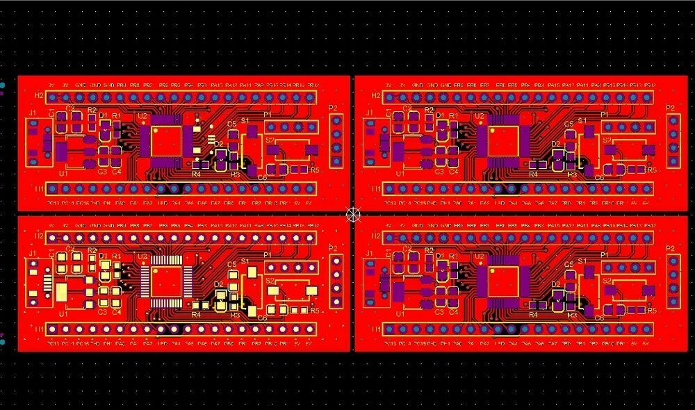
Step 2: Print the PCB Design
Once the schematic design and layout have been completed, the layout is printed onto a special material to form the foundation of the PCB. The material used depends on the type of board being produced and the complexity of the design.
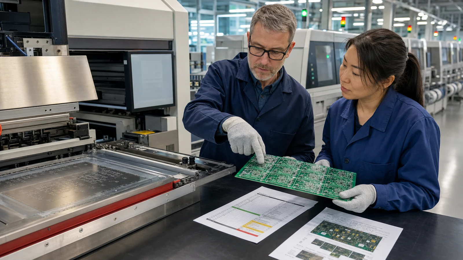
Step 3: Design Review
With the advancement of technology, design reviews have become a necessary pre-production requirement in order to ensure a quality product. The purpose of a design review is to identify and address any potential errors in the design before the start of fabrication. This includes verifying that all components, such as the board outline, board layers, trace widths, drill sizes, and component placement, meet the required specifications. Design reviews also identify any potential manufacturing problems that could affect the cost and quality of the end product. Through the design review process, the quality of the design is improved, and the cost of manufacturing the product is lowered.
Step 4: Inner Layer Imaging
The next step in the PCB manufacturing process is inner layer imaging. This involves taking the printed layout and transferring it onto a copper layer. The copper layer is then put through a photolithography process in which a light sensitive material is applied and then exposed to a light source. This process is then repeated on the other side of the board.

Step 5: Inner Layer Etching
Once the imaging process is completed, the board is then put through an etching process. This involves using a chemical solution to etch away the copper in areas that are not needed for the circuit.

Step 6: Inner Layer AOI
Once the copper has been etched away, the board is then put through an automated optical inspection (AOI) process. This involves using a special machine to inspect the board for any errors.

Step 7: Inner Layer Oxide
After the AOI process is complete, the board is then put through a process of adding an oxide layer. This is done in order to protect the board from corrosion and oxidation.

Step 8: Laminated PCB
The board is then put through a process of lamination. This involves applying a special material to the board in order to strengthen it and increase its rigidity.

The lamination process is critical in ensuring structural integrity, which is why choosing an experienced Multilayer PCB Manufacturer is vital for high-reliability applications.
Step 9: Drilling Holes
Drilling is a key step in the printed circuit board (PCB) fabrication process. It involves creating holes in the board material so that components, such as integrated circuits, can be mounted. The process involves using a drill bit, usually made of high-speed steel or solid carbide, to penetrate the board material. In order to create accurate and reliable holes, the drill bit must be precisely aligned with the PCB. The drilled holes must also be clean and uniform, with minimal surface damage. Additionally, the drilling process must be fast, efficient, and cost-effective. To achieve these goals, various drilling machines and tools are used to control the speed, pressure, and temperature of the drilling process. The use of these machines and tools has enabled PCB manufacturers to optimize the drilling process and produce high-quality boards.

Step 10: PCB plating
PCB plating is a crucial step in PCB (Printed Circuit Board) manufacturing, as it ensures the electrical connections between components are properly established. This process involves applying a thin layer of metal to the PCB, such as copper, to give it conductivity and make it more durable. It also increases the PCB’s ability to withstand extreme temperatures, corrosion, and other environmental conditions.
The most common type of plating used in PCB manufacturing is electroless plating, as it is the most efficient and cost-effective. This process involves using chemicals to plate the PCB with a metal alloy such as copper, nickel, or gold. It also has the additional benefit of providing a protective layer and making the board more reliable.
Another type of plating used in PCB manufacturing is electroplating, which is a more intricate process that involves applying the metal with an electric current. This plating is more expensive and time-consuming, but it is also more precise and provides better protection for the PCB.
Overall, PCB plating is an essential step in PCB manufacturing, as it ensures that electrical connections are proper and that the board is adequately protected from environmental and other factors.

Step 11: Outer layer imaging
The outer layer imaging process is how the circuit layout is transferred onto the board. This process involves taking a CAD layout of the desired circuit and photographing it onto the board.
The imaging process begins with the PCB design being sent to the manufacturer. The design is then photographed onto a film that is the same size as the PCB. The film is then placed onto the PCB, which is etched with a chemical compound to create the circuit traces. The board is then cleaned and inspected to make sure the traces are properly formed.
After the board is inspected, the outer layer is imaged onto the board using a laser or inkjet printer. The imaging process must be precise and accurate so that there are no errors in the trace layout. It is important for the manufacturer to use the best imaging technology available to ensure the highest quality product.
Step 12: Outer layer etching
One of the primary steps in the PCB manufacturing process is outer layer etching, which is also sometimes referred to as subtractive etching.
Outer layer etching is the process of removing excess copper from the board in order to create the desired traces and patterns. This is done by etching away the unwanted copper, leaving behind the desired traces and patterns. The process is done using a chemical etchant, usually a solution of ferric chloride, which eats away the copper that is not protected by the mask.
This process is usually done with a photographic process, where a photoresist is applied to the board. The photoresist is then exposed to a film positive of the desired pattern and the board is developed, leaving the desired patterns exposed to the chemical etchant. The etchant is then used to etch away the exposed copper, leaving behind the desired traces.
Outer layer etching is a critical step in the PCB manufacturing process and can affect the overall performance of the device, as a bad etch can lead to shorts, opens, and other problems. Therefore, it is important to ensure that this step is done correctly and with the utmost care.

Step 13: Outer layer AOI
The outer layer AOI step is an important part of the PCB manufacturing process because it allows for the detection of any errors that may be present on the PCB. This is done by using an automated system that inspects the PCB for any flaws or discrepancies. The system will then flag any areas where there is an issue and make the necessary corrections to ensure that the PCB is of high quality. This process also helps reduce any potential risks associated with the PCBs, as any errors that are detected can be rectified before they cause any problems.
The process of carrying out the outer layer AOI step in PCB manufacturing is relatively simple. First, the PCB is placed onto a conveyor belt and then scanned by a specialized camera. The camera will then detect any flaws or discrepancies that may be present on the PCB. Once this is done, the camera will then flag any areas where there is an issue and the necessary corrections can be made.
The advantages of using the outer layer AOI step in PCB manufacturing are numerous. Firstly, it helps to ensure that the PCBs produced are of high quality and reliable. Furthermore, this process reduces the risk of any problems occurring due to flaws or errors present on the PCBs. Additionally, it also helps to speed up the process of PCB manufacturing by allowing for quicker detection and rectification of any errors that may be present.
In conclusion, the outer layer automated optical inspection (AOI) step in PCB manufacturing is a crucial part of the process. It helps to ensure that any errors are identified and rectified before they cause any problems. Additionally, it also helps speed up the PCB manufacturing process, reducing waste and increasing efficiency.

Step 14: Solder Mask Application
The solder mask application is a critical step in the PCB manufacturing process. It helps to ensure that the electrical connections are protected from contamination and damage due to environmental factors. The application typically involves applying a thin layer of solder mask over the entire board before the components are soldered. This layer helps to ensure that the solder connections remain intact and free from accidental contact with other components, as well as providing insulation from external forces. The solder mask is also used to create a uniform look over the entire board, and it can be used to make it easier to identify components. By using a solder mask in the PCB production process, manufacturers can reduce the risk of product defects while also creating a visually pleasing and consistent product.

Step 15: Legend printing
Legend printing involves printing a wide range of colors on the board to denote different components and designations. By printing on the board, a manufacturer can clearly identify which components are located where, what type of components they are, and any other necessary information. The importance of this step can’t be overstated, as without it, components would be difficult to identify and trace, which could lead to costly errors when assembling and testing the board.

Step 16: Surface treatment
Depending on the application, the surface of the PCB can be subjected to a variety of treatments to ensure its durability and performance. The most commonly used surface treatments are immersion gold, nickel deposition, Hot Air Solder Leveling (HASL), Electroless Nickel Immersion Gold (ENIG), Immersion Silver (ISn), Organic Solderability Preservative (OSP), and Electroless Nickel Electroless Palladium Immersion Gold (ENEPIG).
Immersion gold
Immersion gold is an electroplating process that is used to coat the PCB surface with a thin layer of gold. This layer of gold helps to protect the board from corrosion and oxidation and also provides a better electrical connection and improved solderability. Nickel deposition is also used for the same purpose, but it produces a thicker coating than immersion gold and is more resistant to wear and tear.

Hot Air Solder Leveling (HASL)
Hot Air Solder Leveling (HASL) is a surface treatment that is often used in the assembly of high-reliability printed circuit boards. In this process, the board is exposed to a hot air stream that helps to level out the surface of the board and create a uniform solder coating. This method provides superior solderability and also helps with soldering of lead-free components.

Electroless Nickel Immersion Gold (ENIG)
Electroless Nickel Immersion Gold (ENIG) is a surface treatment that combines the advantages of both immersion gold and nickel deposition. This method creates a thin layer of gold over a thicker layer of nickel, providing superior electrical connection and solderability.
Immersion silver
Immersion silver is a surface treatment that coats the PCB surface with a thin layer of silver. This layer of silver helps to improve the solderability of the board and also provides superior electrical performance.
Organic Solderability Preservative (OSP)
Organic Solderability Preservative (OSP) is a surface treatment that is applied to smooth and level the surface of the board and improve solderability. OSP helps to protect the board from oxidation and corrosion while also providing a better electrical connection.
Electroless Nickel Electroless Palladium Immersion Gold (ENEPIG)
Electroless Nickel Electroless Palladium Immersion Gold (ENEPIG) is a surface treatment that combines the advantages of electroless nickel immersion gold and electroless palladium immersion gold. This method creates a thin layer of gold over a thicker layer of nickel and palladium, providing superior electrical connection and solderability.
Step 17: Electrical test
Electrical test is done to ensure the quality of the printed circuit board created and verify that all components are functioning correctly. During electrical testing, various tests are conducted to make sure the board is performing correctly. This includes continuity testing, insulation testing, current testing, voltage testing, and so on. It is important to note that each test is different and the quality and accuracy of the tests differ based on the product. Electrical testing ensures that there are no faults in the board and that it operates as intended. Electrical testing is one of the last steps in the PCB manufacturing process, so it is important to ensure quality assurance and product safety.

Step 18: Mechanical processing
The mechanical processing step involves cutting and drilling holes in the boards that are needed for components to be placed, as well as other features that may be necessary for the board to function. Machining is a highly precise process, and it requires specialized tools and advanced technologies that can produce highly accurate results. It is important for the machining process to be done correctly, as any mistakes can have a significant impact on the performance of the board. Additionally, machining can involve a number of different processes, each of which can be used to produce different results. The most common processes involve drilling, milling, routing, and laser cutting. Each of these processes has its own advantages and disadvantages and can be used to produce PCBs with different levels of complexity. Machining processing is an essential step in ensuring that the PCBs produced are of the highest quality and are able to meet the needs of the customer.

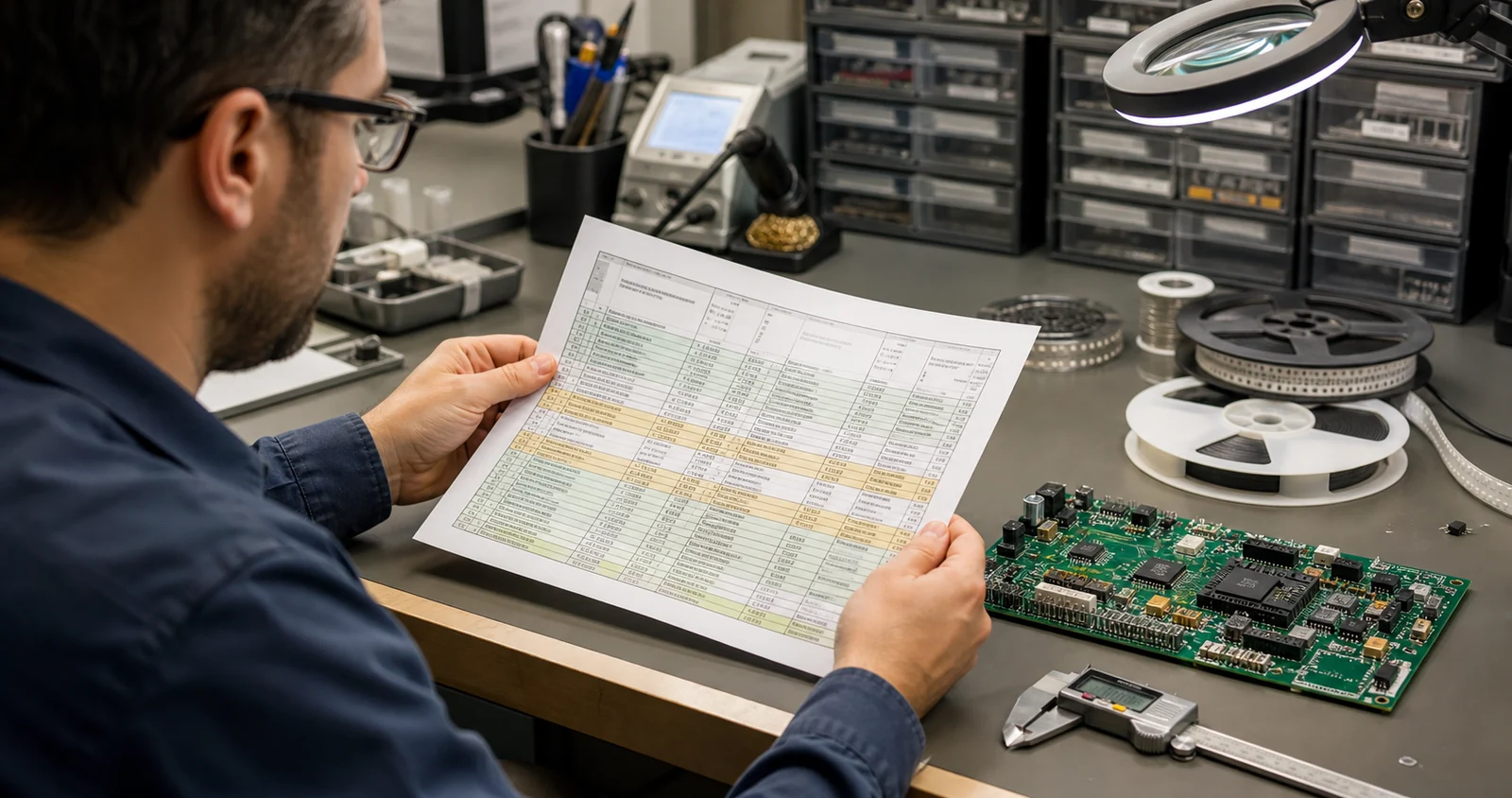
Step 19: Quality inspection and visual inspection
Quality inspection and visual inspection are essential stages of the PCB manufacturing process that ensure the final product meets industry standards and customer expectations. This process involves the careful examination of both the physical attributes and the electrical components of the PCBs.

The quality inspection and visual inspection process is done through a series of tests and evaluations. Here are the requirements for quality inspection and visual inspection:Non any physical defects, such as scratches, dents, burrs, or other deformities.
- Non any electrical defects, such as incorrect soldering, incorrect resistors, or any other issues with the electrical components.
- The PCB must be tested in accordance with industry standards and customer specifications.
- Any issues identified during the inspection process must be documented and addressed.
- Non any potential safety hazards, such as faulty wiring, incorrect voltage levels, or any other potential issues.
- Non any potential performance issues, such as incorrect timing, incorrect signal levels, or any other issues that can affect the performance of the PCB.
- Non for any environmental hazards, such as lead-based solder, or any other hazardous materials.
Step 20: Packaging and delivery
The ultimate step in the fabrication of PCBs is the packing and dispatch. This typically involves a material that wraps around the printed circuit boards in order to protect them from dust and other contaminants, similar to a vacuum packing process. Afterwards, the sealed boards are put into containers which secure them from damage during delivery. Finally, they are sent out to the consumers.
Manufacturing Equipment
The equipment used to manufacture 6-layer PCBs is a laminator, picker, etcher, and a dryer. The laminator is used to cut the boards and adhere to the layers, and the picker is used to remove the boards from the machine. The etcher is used to remove the coating, and the dryer is used to remove the solvent from the board after it is cast.
Materials for manufacturing
The copper stack used for 6-layer manufacturing is 0.4 mm thick, and the copper film is a 0.4 mm thick 1 oz copper. The copper stack used for 6-layer manufacturing is 0.4 mm thick, and the copper film is a 0.4 mm thick 1 oz copper. The laminate used for 6-layer manufacturing is usually FR-0 grade, which is an FR-0 with a 0.33 to 0.35 mm thickness. The laminate used for 6-layer manufacturing is usually FR-0 grade, which is an FR-0 with a 0.33 to 0.35 mm thickness. The dielectric used for 6-layer manufacturing is usually a polyester or a polyimide. The dielectric used for 6-layer manufacturing is usually a polyester or a polyimide. The thermal barrier used for 6-layer manufacturing is usually glass or ceramic. The thermal barrier used for 6-layer manufacturing is usually glass or ceramic.
Tips
– Remember that high volume production is a requirement for 6-layer manufacturing.
– When designing the 6-layer PCB, try to create a standard footprint. This allows for easy board fabrication.
– In order for 6-layer PCBs to meet the requirements of reliable and high performance, the design should be tested. The design should be verified for functionality, and the design should be verified for manufacturability.
– Ensure that the quality of your PCB manufacturing is consistent. It is important to test your boards before you ship them out.
Conclusion
Electronic components such as resistors, capacitors, transistors, diodes, and ICs are becoming smaller and more complex. As a result, the need for reliable and high-quality components is rising. The 6-layer PCB manufacturing process is a low-cost and efficient way to mass-produce these components.