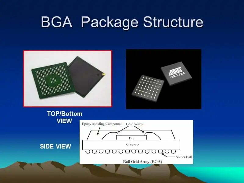
BGA is a commonly used component on PCB, usually CPU, NORTH BRIDGE, SOUTH BRIDGE, AGP CHIP, CARD BUS CHIP, etc. They are mostly packaged in bga type. In short, 80% of high-frequency signals and special signals will be pulled by this type of package. Therefore, how to deal with the routing of the BGA package in the PCB design will have a great impact on important signals.
Types of BGA Parts
The small parts that usually surround the BGA can be divided into several categories according to the priority of importance:
- by pass.
- Clock terminal RC circuit.
(appears in series resistance, row group type; such as memory BUS signal) - EMI RC circuit (appears as dampin, C, pull height; eg USB signal).
- Other special circuits (special circuits added according to different CHIPs; such as CPU temperature sensing circuits).
- Small power supply circuit group below 40mil (appears in the form of C, L, R, etc. This kind of circuit often appears near the AGP CHIP or CHIP with AGP function, and separates different power supply groups through R and L).
- Pull low R, C.
- General small circuit group (appears in the form of R, C, Q, U, etc.; no wiring requirements).
- pull height R, RP.
Routing Rules for BGA Package
The circuits of items 1-6 are usually the focus of placement and will be arranged as close to the BGA as possible, which requires special treatment. Item 7 is the second most important circuit, but it will also be placed closer to the BGA.
Relative to the priority of the importance of small parts near the BGA above, the requirements on ROUTING are as follows:
1. by pass
When it is on the same side as CHIP, directly connect the CHIP pin to the by pass, and then pull it out from the by pass and connect it to the plane; when it is on a different side from the CHIP, it can share the same via with the VCC and GND pins of the BGA, The line length should not exceed 100ml.
2. Clock terminal RC circuit
the requirements of line width, line spacing, line length or including GND; the wiring should be as short and smooth as possible, and try not to cross the VCC separation line.
3. damping
Wire width, wire spacing, wire length, and grouped wiring are required; the wiring should be as short and smooth as possible, and the wiring should not be mixed with other signals.
4. EMI RC circuit
line width, line spacing, parallel lines, GND package, etc. (according to customer requirements.)
5. Other special circuits
Wire width, GND package or wiring clearance and other requirements; according to customer requirements.
6. Small power circuit group below 40mil
wire width and other requirements; try to complete it with the surface layer, reserve the inner space completely for the signal line, and try to avoid the power signal passing through the upper and lower layers in the BGA area, causing unnecessary interference.
7. pull low R, C
no special requirements; smooth wiring.