In the design and reverse engineering of electronic products, pcb layout design is an important step, which directly affects the performance of the circuit. Creating an effective PCB layout is a challenging task, especially if you don’t have enough experience in this field. In this post, you can learn about our pcb layout guidelines to follows all the best practices and standards.
What’s The Ideal PCB Layout?
What exactly is the ideal PCB layout? Well, it’s not a fixed design; it’s an ever-evolving process. Every circuit design is different, and so is the layout. However, there are certain aspects that all successful layouts have in common. Let’s take a look at a few of them.
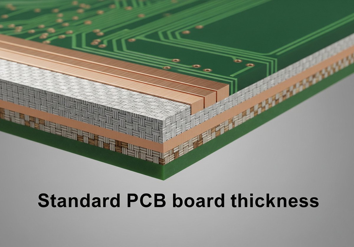
– Trace Width And Length – If you want your circuit to operate properly, you need to make sure that your traces have the proper width and length. This means that you also need to decide where to put them. Width is critical for digital signal integrity. The smaller the width, the less likely it is to pick up noise and interference.
– Ground Placement – The placement of the ground in your circuit design is critical. First, make sure that you have enough ground connections. Next, make sure that they are all connected and to the common analog ground.
– Signal Placement – The placement of the signals in your design is also extremely important. Make sure that the signals are routed in an “inside-out” direction. This means that you start with the most important signals and work your way to the least important ones. If you use a hierarchical chart for the design, this will be much easier.
– Power Distribution – Power distribution is also important. You need to make sure that all the high-power and high-current areas have a connection to the ground. This includes power circuits, as well as high-current traces.
#1 Select Design Strategy Before Layout
Before you start the layout, you need to decide on your design strategy. This includes things like the number of layers, the width of the traces, and the amount of copper you will use. To do this, you need to have a clear idea of what the circuit does and what you need it to do. Furthermore, you also need to know the limitations of the PCB manufacturing process. Below are a few different strategies you can use in the layout of your circuit board:
– Standard Routing – Standard routing is the most common design strategy. You use it when you don’t have any special requirements for your circuit board.
– Micro-Routing – If you need very small traces and very short connections, you will want to use micro-routing.
– Tree Routing – If you need a large number of connections that need to be distributed efficiently, you want to use tree routing. Tree routing is commonly used on high-end boards with a large number of signals.
#2 Establish The Footprint Strategies
After you decide on your design strategy, you need to establish the footprint strategies for your board. You need to decide where you are going to place the components on the board. You need to create a footprint for each component, and you need to place them on the board in a way that makes sense. This includes making sure that the components are placed close to the connections. You don’t want to create a layout that requires the circuit board to be placed in a specific position. This will make it more difficult to assemble and to use the product.
#3 PCB Component Placement Rules
1. interface protection device
For the interface protection device, you should place it as close to the interface as possible. In addition, the different component placement requirement:
The general order of power circuits lightning protection devices: varistors, fuses, suppression diodes, EMI filters, inductors or common mode inductors.
Generally, the order of protection devices for interface signals: ESD (TVS tube), isolation transformer, common-mode inductor, capacitor, and resistor.

2. Components Spacing
Recommended minimum spacing between components:
- The spacing between the edges of the pads of small RC components is >0.3~0.7mm;
- Between other chip components, between SOT, between SOIC and chip components is 1 ~ 1.25mm;
- Between SOIC and between SOIC and QFP is 1.5-2.0mm;
- The distance between PLCC and chip components, between SOIC and QFP is 2-2.5mm;
- 3~4mm between PLCC.
- The distance between the outside of the plug-in component pad and the outside of the chip component pad is greater than 1.5 to 2 mm;
- The edge spacing of the pads between the plug-in components that have been wave soldered is greater than 1 to 2 mm;
- Distance between BGA and adjacent components is greater than 3-5mm.
3. Devices Susceptible to Interference
Devices that are susceptible to ESD interference, such as NMOS and CMOS devices, should be kept away from areas susceptible to ESD interference (such as the edge area of a single board) as far as possible.

4. Clock Device Layout
- Crystals, crystal oscillators and clock distributors should be as close as possible to related IC devices;
- The filter of the clock circuit (try to use the “∏” type filter) should be close to the power lines input pin of the clock circuit;
- Whether the output of the crystal oscillator and the clock distributor is connected in series with a 22 ohm resistor;
- Whether the unused output pins of the clock distributor are grounded through resistors;
- The layout of crystals, crystal oscillators and clock distributors should be kept away from high-power components, heat sinks and other heat-generating devices;
- Whether the crystal oscillator is more than 1 inch away from the edge of the board and the interface device.

5. Capacitors and Filters
- The capacitor must be placed close to the power pin, and the smaller the capacitance, the closer to the power pin;
- The EMI filter should be close to the input port of the chip power supply;
- In principle, each power pin has a small capacitor of 0.1uf and one or more large capacitors of 10uf for an integrated circuit, which can be increased or decreased according to the specific situation.

#4 PCB Routing Rules
PCB routing rules are the guidelines that designers use to determine the placement and routing of tracks on a printed circuit board. These rules help to ensure that the finished PCB will function correctly and meet all the required electrical specifications. There are a variety of different routing rules that can be used, and the specific rules that are followed will depend on the particular design and the requirements of the project.
1. Trace, Signal, and Power connection
There are a few key things to keep in mind when routing PCBs:
– Make sure your trace widths are appropriate for the current you’ll be carrying. Too narrow of a trace will result in excessive heat and potential failure; too wide of a trace will be unnecessarily expensive.
– Be aware of the different types of copper planes and how they can be used to your advantage. Power and ground planes, for example, can be very helpful in keeping noise and crosstalk to a minimum.
– Make sure you take into account the different impedance requirements of digital and analog signals. Digital signals need to be routed with low-impedance traces to minimize reflections and crosstalk, while analog signals can be routed with thicker, higher-impedance traces.
– Pay attention to the spacing between traces, especially when routing high-speed signals. The spacing between traces affects the capacitance of the traces, which in turn affects the signal integrity.
– Consider using vias to route signals between different layers of the PCB. This can be helpful in minimizing the length of the traces and reducing crosstalk.
– Make sure you have adequate clearance around power and ground pins. These areas can be susceptible to arcing and thermal issues, so it’s important to keep them clear.
By following these simple guidelines, you can ensure that your PCBs are properly routed and will function as intended.
2. Kelvin connection
Kelvin connections, also known as force and sense connections, are a convenient way to eliminate the effects of voltage drops on wires in circuits.
Although on a schematic it may look the same placing the connection on a resistor pad or some arbitrary point, the actual trace has inductance and resistance and can cause your measurements to fail if you don’t use a Kelvin connection.

#5 Heating Issure
1. Thermal layout
There are three main aspects of heat in PCB:
- heat sinking through the component plates;
- the heat of the PCB itself;
- heat from other parts.

Placing extra copper around surface mount components provides additional surface area to dissipate heat more efficiently. Some component datasheets (especially power diodes and power MOSFETs or voltage regulators) have guidelines for using the PCB surface area as a heat sink.
2. Thermal Vias and Thermal Relief
Vias can be used to transfer heat from one side of the PCB to the other. This is especially useful when the PCB is mounted on a heatsink on a chassis that can further dissipate heat. Large vias transfer heat more efficiently than small vias. Many vias transfer heat more efficiently than one via and reduce the operating temperature of the component. Lower operating temperatures help improve reliability.

Thermal relief makes connections between traces or padding and component pins smaller to make wave soldering process easier. This small connection is short to reduce the effect on resistance. If you don’t use the heat sinks on the pins of the components, the components may be cooler because there are better thermal connections to traces or fillers that can dissipate heat, but it will be harder to solder and desolder.
#6 Verify Your Layout by Design Rules
After pcb layout have been finished, it’s important to ensure your electrical rules check (ERC) and design rules check (DRC) to verify you’ve met all of your established constraints. They make it simple to specify gap widths, trace widths, common manufacturing requirements, high-speed electrical requirements, and other physical requirements for your particular application.

DRC checking is the program within EDA software that is responsible for checking the design against the rules defined within the software. It’s the last chance to catch design issues before the manufacturing process begins.
PCB Layout Mistakes To Avoid
There are many common mistakes that people make on pcb design guidelines. However, if you avoid these, you will have a much better chance of creating a layout that follows industry standards, is easy to assemble, and has a low chance of failure. Let’s take a look at the most common mistakes that people make when designing a PCB layout.
– Crossing Traces – One of the biggest mistakes that people make when designing a PCB layout is crossing traces. You want to avoid this at all costs. If you create a trace that crosses another trace, it will cause a short circuit.
– Extra Long Traces – You also want to avoid creating traces that are much longer than they need to be. This will make your layout less efficient, and it can cause problems if the trace is too long.
– Short, Distributed Traces – Another mistake that people make is creating a large number of short traces connected to each other in a way that creates an “island.” This is inefficient and can cause problems.
– Missing Ground Placement – You also want to make sure that you have a proper ground placement in your design. This includes making sure that all the nets are connected to the ground plane.
– Having Too Many Power Planes – Another common mistake is creating too many power planes. This is particularly common in high-end designs. However, more power planes will add to your cost and complexity.
Tools For PCB Layout
As you can see, creating a successful PCB layout is a challenging task. You need to take into consideration many different factors, and you need to know how to solve many different types of problems. You also need a few different tools to help you. Here are a few of the most important ones.
– Schematic – The schematic for your circuit determines what your PCB layout will look like. If you get the schematic wrong, you will get the PCB layout wrong. You need to be careful when creating the schematic. The more complicated the circuit, the harder it is to create a correct schematic.
– CAD system – This is a process for designing printed circuit boards. The outline of a printed circuit board is laid out according to requirements. Various symbols are used to represent different components on the board. The outline of the board is then converted into a computer-aided manufacturing (CAM) file. The computer-aided design (CAD) software used for this purpose has the capability to import and export CAM files.
Engineering checks for PCB Layout Guidelines For A Successful Design
Before using PCB Layout Guidelines For A Successful Design in a PCB, firmware, repair, or validation workflow, confirm the details that usually decide whether the design works reliably instead of only reading the headline specification.
Design and troubleshooting checklist
| Area | What to check | Why it matters |
|---|---|---|
| Power and clock | Check rails, decoupling, reset, oscillator, boot pins, and debug access | MCU boards fail quickly when support circuits are weak |
| Firmware path | Match rs485 pcb layout guidelines with toolchain version, memory map, fuses, option bytes, and bootloader flow | Programming assumptions affect recovery and production |
| Validation | Test GPIO, ADC, timers, serial buses, current draw, and fault recovery | Peripheral tests reveal schematic and firmware mismatches |
These checks help connect the search intent around rs485 pcb layout guidelines with practical board-level decisions, component selection, and failure analysis.
Conclusion
Creating an effective printed circuit board layout is a challenging and complicated task. If you are not careful, you can make a lot of mistakes and waste a lot of time. However, by following these PCB layout guidelines, you can create a sound design. One that is easy to assemble and has a low chance of failure.
FAQ
- Impedance matching of signal lines;
- Spatial isolation from other signal lines;
- For digital high frequency signals, differential lines work better.
No, the decoupling capacitors need to be added with appropriate values at appropriate locations. And need to use different capacitance values to filter out spurious signals of different frequencies.
Blind vias can increase the density of multilayer boards, reduce the number of layers and board size, and greatly reduce the number of plated through holes.
However, in comparison, through-holes are easy to implement in terms of technology and have a lower cost, so through-holes are generally used in designs.
The analog circuits and digital circuits should be placed in separate areas so that they do not affect each other.
When laying out a multi-layer board, make sure do not have floating ground or power planes, because power and ground planes are on the inner layer.
In addition, make sure that the vias punched to the ground are indeed connected to the ground plane, so that some test points can be added for some important signals, which is convenient for measurement during debugging.