This comprehensive PCB markings guide provides a complete PCB abbreviations list and circuit board codes used to identify pcb component labels during assembly and troubleshooting.
Printed circuit boards, or PCBs, are a vital component of electronic devices, as they provide a platform for electrical components to be connected and communicate. To ensure that the PCBs are installed and laid out correctly, various markings are used to indicate where specific components should be placed. There are approximately 140 common PCB markings, each with its own distinct meaning. Understanding the purpose of these markings is essential to getting the most out of a PCB. With this knowledge, you can ensure that your PCB is laid out correctly and that all components are installed in the right places.
Meaning of the Different PCB Markings
*Table 1: This comprehensive PCB code list provides 140 circuit board abbreviations and component codes used in electronic design.
| No. | Letters Code | Meaning |
|---|---|---|
| 1 | AAT | automatic power-on device |
| 2 | AC | alternating current |
| 3 | ANT | Antenna |
| 4 | BATT | Battery |
| 5 | BHBM | Temperature measurement sensor |
| 6 | BL | Liquid level sensor |
| 7 | BT1BK | Time measuring sensor |
| 8 | BV | speed changer |
| 9 | C | Capacitor |
| 10 | CN | Connector |
| 11 | D | Diode |
| 12 | DC | direct current |
| 13 | EUI | electromotive voltage current |
| 14 | F | frequency |
| 15 | FB | Ferrite Bead |
| 16 | FET | Field Effect Transistor |
| 17 | FF | Dropout fuse |
| 18 | FL | Filter |
| 19 | FR | thermal relay |
| 20 | FTF | Fast Fuse |
| 21 | FU | fuse |
| 22 | FV | Voltage limiting protection device |
| 23 | G | generator |
| 24 | GDT | Gas Discharge Tube |
| 25 | GND | Ground / Common |
| 26 | HA | Acoustic signal |
| 27 | HB | blue light |
| 28 | HG | Green light |
| 29 | HL | Indicator light |
| 30 | HP | light plate |
| 31 | HR | Red light |
| 32 | HS | Optical signal |
| 33 | HW | White light |
| 34 | HY | Yellow light |
| 35 | IC | Integrated Circuit |
| 36 | J | Jumper / Connector |
| 37 | JK | Jack |
| 38 | JP | Jumper Pin |
| 39 | K | relay |
| 40 | KA | momentary relay |
| 41 | KD | differential relay |
| 42 | KF | flasher relay |
| 43 | KH | thermal relay |
| 44 | KI | impedance relay |
| 45 | KM | intermediate relay |
| 46 | KOF | export intermediate relay |
| 47 | KP | Polarization Relay |
| 48 | KR | Reed Relays |
| 49 | KS | signal relay |
| 50 | KT | time relay |
| 51 | KV | voltage relay |
| 52 | L | Inductor / Line |
| 53 | LED | Light Emitting Diode |
| 54 | M | Motor |
| 55 | MIC | Microphone |
| 56 | MOD | Module |
| 57 | MOV | Metal Oxide Varistor |
| 58 | NC | Not Connected |
| 59 | OSC | Oscillator |
| 60 | PA | Ammeter |
| 61 | PAR | Reactive ammeter |
| 62 | PF | Frequency table |
| 63 | PJ | Active energy meter |
| 64 | PJR | Reactive energy meter |
| 65 | PM | Maximum Demand Meter (Load Monitor) |
| 66 | PPA | Phase Meter |
| 67 | PPF | Power Factor Meter |
| 68 | PR | Reactive power meter |
| 69 | PW | Active power meter |
| 70 | PQS | active and reactive apparent power |
| 71 | Q | circuit switching device |
| 72 | QF | circuit breaker |
| 73 | QS | isolation switch |
| 74 | R | Resistor |
| 75 | REL | Relay (Generic) |
| 76 | RT | Thermistor |
| 77 | RV | Varistor |
| 78 | SA | transfer switch |
| 79 | SB | push button switch |
| 80 | SBE | Panic button |
| 81 | SBP | Pressure switch |
| 82 | SBR | Reverse button |
| 83 | SBS | Stop button |
| 84 | SBT | Test button |
| 85 | SC | Contactor |
| 86 | SCR | Silicon Controlled Rectifier |
| 87 | SE | experiment button |
| 88 | SG | Signal lamp |
| 89 | SL | Level switch |
| 90 | SM | Humidity control switch |
| 91 | SP | Pressure control switch |
| 92 | SPK | Speaker |
| 93 | SQ | Limit switch |
| 94 | SQP | Proximity switch |
| 95 | SR | Reset button |
| 96 | SS | Speed control switch |
| 97 | ST | Temp control auxiliary switch |
| 98 | SV | Voltmeter changeover switch |
| 99 | SW | Automatic transfer switch |
| 100 | T | Transformer |
| 101 | TA | current transformer |
| 102 | TBP | Pressure transmitter |
| 103 | TC | Thermocouple |
| 104 | TF | Temperature limiter |
| 105 | TG | Thermostat |
| 106 | TH | Heater |
| 107 | TM | Temperature transmitter |
| 108 | TP | Test Point |
| 109 | TR | Thermoresistance |
| 110 | TT | Temperature controller |
| 111 | TV | voltage transformer |
| 112 | U | Rectifier / Integrated Circuit |
| 113 | UB | Uninterruptible power supply |
| 114 | UC | Converter |
| 115 | UI | Inverter |
| 116 | UR | Thyristor rectifier |
| 117 | US | Soft starter |
| 118 | UT | Step-down transformer |
| 119 | V | Frequency converter |
| 120 | VC | Control circuit with power rectifier |
| 121 | VR | Variable Resistor / Potentiometer |
| 122 | W | Cable / Wire |
| 123 | WB | DC bus |
| 124 | WC | Control small busbar |
| 125 | WCL | Closing small busbar |
| 126 | WE | Emergency lighting branch line |
| 127 | WELM | Emergency Lighting Small Busbar |
| 128 | WEM | Emergency lighting mains |
| 129 | WF | Flash small busbar |
| 130 | WFS | Accident Sound Small Bus |
| 131 | WIB | Plug-in (feed) bus |
| 132 | WL | Lighting branch line |
| 133 | WLM | Lighting mains |
| 134 | WP | Power branch line |
| 135 | WPM | Power mains |
| 136 | WPS | Forecast audio small bus |
| 137 | WS | Signal small busbar |
| 138 | WT | trolley line |
| 139 | WV | Voltage small busbar |
| 140 | Y | Crystal Oscillator |
Reference guide: PCB component codes and abbreviations list (Optimized for technical printing). Size: 150KB
How are PCB Markings and Component Labels Applied?
Understanding how PCB marking is executed during the manufacturing process is crucial for ensuring durability and readability. Depending on the density of the board and the required precision, several industry-standard methods are used to apply pcb component labels and circuit board markings.
1. Silkscreen Printing (The Industry Standard)
Silkscreen is the most common method for applying a PCB markings guide to a board. It involves pushing specialized ink through a stencil (screen) onto the PCB surface.
Best for: Standard component marking and large logos.
Advantage: Cost-effective for high-volume production.
Limitation: Lower resolution compared to digital methods, making it difficult for extremely high-density layouts.
2. Liquid Photo Imaging (LPI)
LPI uses a process similar to the application of solder mask. A photo-imageable epoxy is coated onto the board, exposed to UV light through a film, and then developed. This provides higher accuracy for pcb board abbreviations and fine lines than traditional silkscreen.
3. Laser Marking (Micro Marking on Electronic Copper)
For high-end or high-density boards, micro marking on electronic copper or the substrate is achieved using high-precision UV or CO2 lasers.
Precision: This method is essential for tracking individual boards with tiny DataMatrix codes or serial numbers.
Durability: Unlike ink, laser-etched circuit board markings are permanent and resistant to harsh chemicals and high heat during the reflow process.
4. PC Marking Thermal Transfer Printing
When variable data is required—such as unique tracking IDs or date codes—pc marking thermal transfer printing is often employed.
The Process: A thermal print head melts a wax or resin ribbon onto a heat-resistant label, which is then applied to the PCB.
Application: Ideal for pcb component labels that need to be updated frequently without redesigning the entire silkscreen layer.
Comparison of Marking Technologies
*Table 2: Comparison of different technologies used for pcb marking and identifying pcb component codes.
| Marking Method | Precision Level | Durability | Best Use Case |
|---|---|---|---|
| Silkscreen Printing | Medium Precision | High | Standard pcb component marking and logos. |
| Laser Etching | Ultra-High Precision | Permanent | Micro marking on electronic copper for high-density tracking. |
| Thermal Transfer | High Precision | Medium | Variable pcb component labels and unique serial numbers. |
| Direct Inkjet (LDI) | High Precision | High | Complex circuit board markings and quick-turn prototypes. |
Tips for Reading PCB Markings
Reading the markings on a printed circuit board (PCB) can be daunting at first, but with some practice and basic knowledge of the symbols and codes used, it can become second nature. Here are some tips to help you get started:
1. Learn the basic symbols and codes
Familiarize yourself with the most common symbols and codes used on PCBs, such as component designators, polarity indicators, reference designators, and rating markings. Knowing these will help you understand the information on the board more easily.
2. Read the component labels
Component labels usually include a manufacturer’s part number, a description of the component, and the electrical characteristics of that component. This information will help you identify what type of component is installed on the board and its specifications.
3. Inspect the board closely
Take your time when inspecting the board to look for any signs of damage or corrosion. Look for any solder joints that may have been disturbed, and any components that may have been added or removed from the board. Learning how to identify and fix issues like cold solder joints can be very helpful.
4. Refer to the schematic
If you’re having trouble understanding the markings on the board, refer to the schematic to cross-reference the markings and make sure they match up. This can help you determine if there are any discrepancies between the board and the schematic.
5. Test the components
Once you’ve identified the components on the board, test them to make sure they’re working correctly. This will help you confirm that the board is functioning properly and is free of defects.
6. Read the markings from left to right
When reading a PCB marking, it is important to read the markings from left to right, as this will help to ensure accuracy. This is especially important when there are multiple components in a single line.
7. Look for additional information
In some cases, additional information may be included on the PCB markings. For example, the maximum voltage or current rating of a component may be included. It is important to look for this information in order to ensure that the component is suitable for its intended purpose.
8. Use a reference guide
If you are having difficulty interpreting a PCB marking, it can be helpful to consult a reference guide. A reference guide will provide detailed information about the various symbols and abbreviations used in PCB markings, as well as their meaning.
Frequently Asked Questions about Circuit Board Markings
Q1: What is the most common PCB abbreviations list for components?
Most manufacturers follow the IPC-2612 standard. Common pcb component codes include ‘R’ for resistors, ‘C’ for capacitors, and ‘U’ for integrated circuits. Our table above serves as a quick pcb board abbreviations reference for these identifiers.
Q2: How is micro marking on electronic copper achieved?
Micro marking on electronic copper is typically achieved through high-precision laser direct imaging (LDI) or specialized etching. For serial numbers, pc marking thermal transfer printing is often used on heat-resistant labels that are then applied to the board.
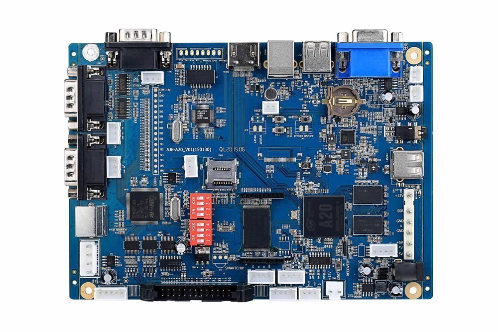
Engineering checks for PCB markings, reference designators, and inspection codes
Before using PCB markings, reference designators, and inspection codes in a PCB, firmware, repair, or validation workflow, confirm the details that usually decide whether the design works reliably instead of only reading the headline specification.
Design and troubleshooting checklist
| Area | What to check | Why it matters |
|---|---|---|
| Reference designators | Check R, C, L, D, Q, U, J, TP, F, and polarity marks against the BOM | Markings speed repair only when they match the schematic |
| Manufacturing marks | Record UL, date code, RoHS, panel, assembly, and revision identifiers | Board history helps failure analysis and counterfeit detection |
| Inspection | Verify silkscreen clearance, pin 1 marks, test-point labels, and connector orientation | Readable markings reduce assembly and service mistakes |
These checks help connect the search intent around PCB markings guide with practical board-level decisions, component selection, and failure analysis.
PCB labeling review checklist - PCB labeling
This PCB labeling review checklist helps engineers review PCB labeling with focus on reference designators, polarity marks, pin 1 indicators, test point labels, assembly notes, and service markings before the design is released to fabrication or system validation.
Practical checklist
- Keep component reference designators readable after solder mask, silkscreen clipping, and assembly clearance checks.
- Use clear polarity and pin 1 indicators for connectors, diodes, electrolytic capacitors, and IC packages.
- Align test point labels with the schematic so troubleshooting and reverse engineering remain repeatable.
FAQ
When should PCB labeling be checked? Check PCB labeling before layout freeze and again after real bench measurements.