Vias are the critical vertical pathways that transform a simple board into a complex, multi-layered electronic marvel. This guide explores their types, design principles, and manufacturing intricacies.
Anatomy of a Via
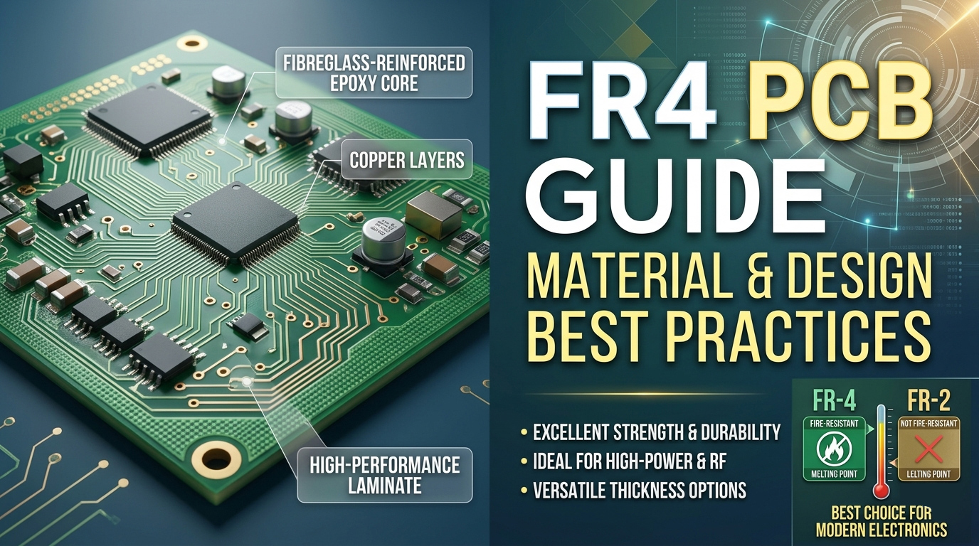
A via, short for Vertical Interconnect Access, is a tiny, copper-plated hole that creates an electrical connection between different layers of a Printed Circuit Board. It's essential for routing signals and power in modern, dense electronics.
- Barrel: A conductive tube used to fill the drilled hole.
- Pad: Connects the ends of the barrel to the traces.
- Antipad: A gap used to separate non-connected layers and the barrel.
The Via Family: A Look at Different Types
From the common through-hole to the microscopic microvia, each type offers a unique trade-off between cost, space, and performance. The choice of via is a critical design decision.
🔩 Through-Hole Via
Connects all layers, from top to bottom. Simple and low-cost, but consumes significant board space.
👁️ Blind Via
Connects an outer layer to one or more inner layers. Saves space and is key for HDI designs.
🧱 Buried Via
Connects only inner layers and is invisible from the outside. Maximizes surface area for components.
🔬 Microvia
Extremely small vias used for HDI PCBs. Enables routing of fine-pitch components and improves signal integrity.
🎯 Via-in-Pad
Placed directly on a component's pad. Great for thermal management and miniaturization, but increases cost.
🚦 Stacked & Staggered
Stacked vias are vertically aligned for higher density, while staggered vias are offset for improved reliability.
Functions of PCB Vias
PCB vias serve various functions in electronic circuits, playing a crucial role in the board's overall performance and integrity.
Signal Routing
Vias facilitate the path for signals to traverse between different signal layers, allowing components on one side of the board to communicate with those on the other side.
Power Distribution
Vias play a vital role in distributing power and ground connections between different layers, ensuring a stable power supply to all components.
Escape Routing
Larger surface mount (SMT) components mostly use through holes for escape routing. Microvias or blind vias are most commonly used for escape routing, but via-in-pad can be used in solid packages such as high pin count BGAs.
Component Connection
Through holes or blind holes can be used to provide multiple connections to the plane. For example, a strip of metal with stitched vias surrounds sensitive areas of the circuit, connecting it to the ground plane for EMI protection.
Heat Conduction
Vias can be used to conduct heat outward from the internal planar layers through which components are connected. Typically, thermal vias require dense blind or via holes that must be located in the pads of these devices.
Via Comparison: Cost vs. Density
This chart visualizes the fundamental trade-off in via selection. As density requirements increase (moving right), so do the manufacturing complexity and cost (moving up). Microvias offer the highest density at the highest cost.
Critical by Design: Key Rules & Considerations
Aspect Ratio
≤10:1
The ratio of via depth to its diameter. A lower ratio is crucial for reliable copper plating and preventing stress cracks.
Annular Ring
≥1mil
The copper pad around the via. A sufficient ring ensures a solid connection even with minor drill misalignment.
Advanced Challenges
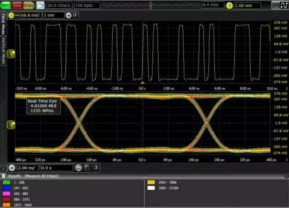
Signal Integrity
Vias can act like tiny antennas, causing reflections and degrading high-speed signals. Proper design, including minimizing stubs and using ground vias, is essential.
Thermal Management
Vias are key pathways for heat to escape from components. Filled thermal vias under hot components prevent overheating and improve reliability.
The Making of a Via: Manufacturing Flow
Creating a reliable via is a multi-step process requiring immense precision. From drilling the initial hole to the final plating, each stage is critical to the PCB's performance.
Drilling
Laser or mechanical drills create precise holes through the PCB layers.
Metallization
A thin layer of copper is chemically deposited to make the hole walls conductive.
Plating
Additional copper is electroplated to thicken the connection for robustness.
PCB Via Processing
To improve PCB assembly yield or thermal performance, the vias are often subject to additional processing, including filling, capping, tenting, or covering.
Tented Via
Tented Via involves covering both ends of a via with non-conductive solder mask, effectively sealing the opening. This is popular when using dry film solder mask layers, as it effectively covers large holes without cracking.
Plugged Via
Plugged Via uses non-conductive epoxy resin to fill one or both ends of the via, preventing solder from flowing through during the soldering process. For effective plugging, the via’s diameter is typically limited to a maximum of 20 micrometers. Manufacturers often use solder mask layers to cover plugged vias.
Filled Via
Manufacturers may use non-conductive epoxy resin paste to fill regular or intruded vias. These filled vias are positioned a few micrometers away from the pads. For medium-density PCBs, this is a good compromise, as the presence of solder mask layers reduces the likelihood of solder bridging between vias and adjacent pads.
Conductive Filled Via
Some manufacturers use conductive paste to fill microvias, enhancing their conductivity. This filling can be epoxy resin mixed with copper or, in some cases, pure copper.
Common Pitfalls & Solutions
Even with the best designs, manufacturing issues can arise. Understanding these common problems and their solutions is key to producing high-quality, reliable boards.
Solutions
Solder Wicking
Prevent solder from being drawn into the via by applying via tenting or plugging during manufacturing.
Structural Cracking
Ensure the aspect ratio is within acceptable limits (≤10:1) and select appropriate materials for thermal expansion.
Signal Integrity Issues
Mitigate signal degradation in high-speed designs by using back-drilling to remove via stubs or placing ground vias nearby.
Incorrect Plating
Adhere to strict manufacturing process controls, including proper cleaning and electroplating to ensure robust copper deposition.
Misalignment
Maintain a sufficient annular ring size in your design and use high-precision drilling equipment to minimize drilling inaccuracies.
Frequently Asked Questions
1. How to choose the size (diameter) of a via?
The size depends on PCB layer count, current magnitude, signal frequency, and manufacturing processes:
- Small diameters (e.g., 0.2–0.5mm) suit high-frequency signals and dense layouts, reducing parasitic effects.
- Larger diameters (e.g., 0.8mm+) are used for high-current transmission (e.g., power/ground) to lower resistance and heat generation.
- Always confirm the minimum manufacturable size with your PCB manufacturer (limited by drilling and plating capabilities).
2. Can vias be used for heat dissipation?
Yes. Large-diameter vias or densely arranged vias help conduct heat from inside the PCB to the surface or heat sinks, particularly near power devices (e.g., chips, MOSFETs). Metal-filled vias (e.g., with copper) are sometimes used to enhance heat dissipation.
3. What common mistakes should be avoided in via design?
- Insufficient via spacing, leading to drilling deviations or short circuits during manufacturing.
- Poor connection between signal vias and ground planes, causing EMI (electromagnetic interference).
- Neglecting solder mask design for vias, resulting in solder flowing into holes and causing shorts.
- Using undersized vias for high-current scenarios, leading to overheating and burnout.
4. Are blind and buried vias more expensive to manufacture?
Yes. Compared to through-hole vias, blind and buried vias require more complex processes (e.g., laser drilling, pre-processing before lamination), increasing manufacturing costs. They are suitable for space- and performance-critical applications (e.g., smartphone or drone PCBs).
5. Can vias be non-plated?
No. Non-plated vias cannot conduct electricity and lose their function of connecting layers. Plating (usually copper) is essential for vias to achieve electrical conduction, requiring uniform, void-free plating on hole walls.
6. How to test via reliability?
Common methods include:
- Continuity testing (to check effective layer-to-layer connection).
- Impedance testing (to verify impedance matching in high-frequency signals).
- Thermal cycle testing (to simulate high-low temperature environments and evaluate plating fatigue resistance).
- Pull testing (to assess the bonding strength between vias and pads).
7. What are the future trends in via technology?
- Miniaturization: As PCBs become more dense, via diameters are shrinking to the micrometer range (e.g., 50–100μm), relying on laser drilling.
- New Materials: Adoption of advanced conductive materials (e.g., graphene) to improve conductivity and heat dissipation.
- 3D Integration: Integration with IC packaging technologies (e.g., extending TSV silicon via technology) for more compact interlayer connections.