
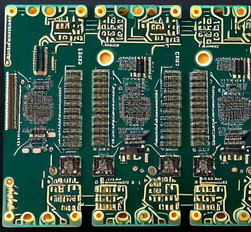
LED PCBs Explained: Design & Functionality
Understand LED PCBs: types (FR4, aluminum), thermal management, and soldering. Tips for LED layout and driver integration. Ideal for lighting projects. Guide here!
Understand LED PCBs: types (FR4, aluminum), thermal management, and soldering. Tips for LED layout and driver integration. Ideal for lighting projects. Guide here!
FR4 PCB material: properties, thickness, and cost-effectiveness. Tips for designing single/double-layer boards. Ideal for most applications. Ultimate guide inside!

HDI (High-Density Interconnect) PCBs: layers, microvias, and advanced manufacturing. Ideal for mobile devices and wearables. Expert insights inside!

Build PCB libraries: component footprints, symbols, and 3D models. Tools for Altium/KiCad and version control. Essential for efficient design. Tutorial inside!

Master PCB BOM creation: component listing, part numbers, and sourcing. Tips for accuracy, cost optimization, and manufacturability. Download template inside!

What is PCB Footprint? PCB footprint, is the arrangement of pads used to mount a specific component to a printed circuit board. The footprint defines the outline of the component and the location of the mounting pads. It’s an important

Master PCB layout: trace width, ground planes, and component placement. Tips for signal integrity, thermal management, and manufacturability.

The adoption and implementation of 5G connectivity are underway, as mobile carriers race to be the first company with a 5G network. A key enabler of 5G is low latency, high bandwidth, and high cell density. These three capabilities require

Gerber files for PCBs: formats, layers, and why they’re critical for manufacturing. Learn to generate and verify files with Eagle/Altium. Step-by-step guide!
PCB designers need to understand PCB trace basics to create high-performance printed circuit boards. From basic definitions to the types of traces, this article covers all the fundamentals you need. Working with printed circuit board (PCB) design software can be