High density interconnect (HDI) printed circuit board is an electronic circuit board that has high-density metal traces, i.e., it has more copper per unit area than conventional PCBs. These boards are used for high-frequency pcb and high-density connections in electronics. They are also known as double-sided interposer boards, HDI boards, or HDIP boards.
What Is HDI Printed Circuit Board?
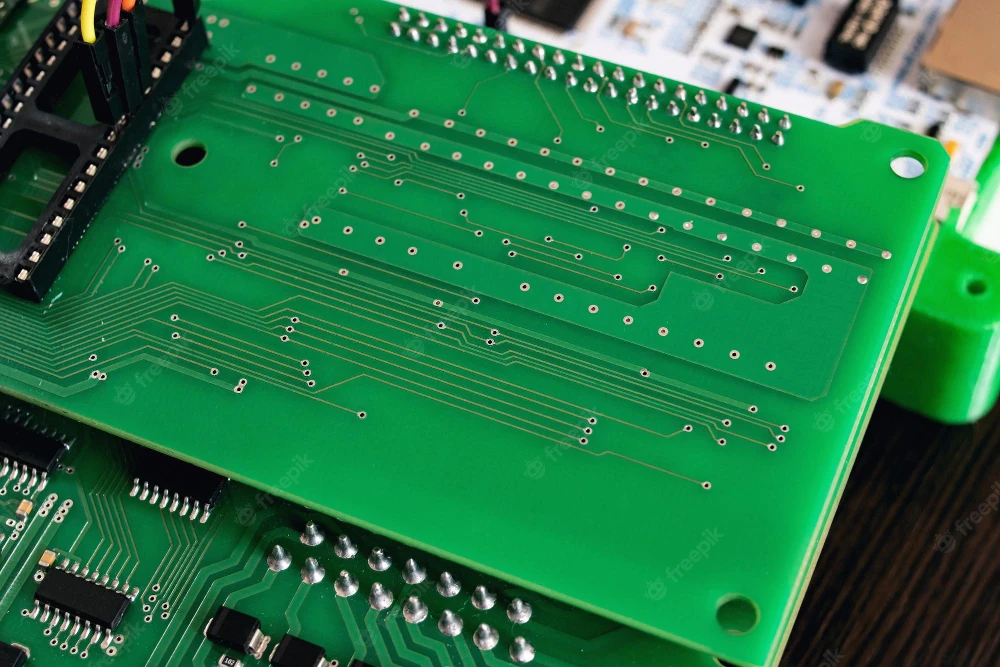
HDI printed circuit boards are like normal printed circuit boards, but with two significant additions. The first is that there are higher-density copper traces, meaning that there is more copper per unit area than in conventional PCBs. The other difference is that the two sides of the board are laminated together, forming a sandwich with no air gaps between layers. The board may be sandwiched between metal plates, or a hollow-core board may be used. The metal plates are used to provide a ground plane to shield the circuit from electromagnetic interference (EMI). The ground plane also provides electrostatic protection against electrostatic discharge, which can destroy sensitive electronic components. The shielding also prevents capacitive coupling between circuits, which can cause noise in nearby circuits.
Types of HDI PCBs
HDI board can be divided into first-order, second-order, third-order, fourth-order, fifth-order, etc. according to the number of layers of blind hole plating. In the PCB industry, the 1st-order HDI board is also called “1+n+1”, and the 2nd-order HDI board called “2+n+2”, as shown in the figure.
1+n+1
The structure of the first-order HDI board is relatively simple, and the process is relatively easy to control. The pink holes in the picture are blind holes, which are made by laser drilling, and the diameter is usually 3 ~ 4 mil; the yellow holes are buried holes, which are made by mechanical drilling, and the diameter is at least 6 mil (0.15 mm) or more.

2+n+2
There are various structures of the second-order HDI board. One is that the positions of each order are staggered, and the adjacent layers need to be connected in the middle layer through wires. This approach is equivalent to two first-order HDIs. The second is that the two first-order holes are overlapped, and the second-order is realized by superimposing, and the processing is similar to the two first-orders. The third is to punch directly from the outer layer to the third layer (or N-2 layer). The process is very different from the previous one, and the difficulty of punching is also greater.

HDI Boards vs Through Hole Board
Multilayer circuit boards usually include through-hole boards, first-order boards, second-order boards, and second-order stacked orifice boards. Their structures are compared as follows:

1. through-hole Board
There is no direct relationship between the through-hole plate and the number of layers. It is connected from the first layer to the last layer. The inner diameter of the through-hole is usually 0.2mm, 0.25mm and 0.3mm. The 0.2mm is much more expensive than 0.3mm. Because the 0.2mm drill is too thin and easy to break.

2. First-order HDI Board
This is a stack structure diagram of a 6-layer 1st-order HDI board. The two layers on the surface are laser holes with an inner diameter of 0.1mm. The inner 4 layers are mechanical holes, similar to through holes.
The laser can only penetrate the glass fiber plate, not the metal copper. So punching holes on the outer surface will not affect other circuits inside. After the laser has drilled the hole, copper is plated to form a laser via.

3. Second-order HDI board (staggered hole)
This is a 6-layer 2-order staggered hole HDI board, with 2 layers of laser holes on the upper and lower sides and separated from each other.

4. Second-order HDI board (stacked hole)
The two layers of laser holes of the staggered hole board are overlapped to form a stacked hole HDI board. The inner laser hole is filled with electroplating, and then the outer laser hole is made.

The Development Of HDI PCB
The first HDI PCB assembly was developed by the Boeing Aircraft Company, who needed a new way to mount printed circuit boards to their aircraft during World War II. Since the PCBs are sandwiched between two metal plates, the interconnects between the plates can be very close together. This allowed the engineers to use short interconnects, and create circuitry with more density and higher frequencies. The first commercial HDI PCB assembly was used by the Collins Radio Company in 1962. With the development of very high frequency (VHF) and ultrawideband (UWB) RF products, the demand for HDI technologies has increased significantly in the last few years.
HDI PCB Application
High-density interconnect PCBs are used in high-frequency and high-density connections in electronics. They are also used for interconnects in power electronics. Some of the applications for these boards are:
- mobile phones, smartphones, digital cameras;
- wireless LAN modules, GPS modules, audio chipsets;
- communication devices in satellites/aerospace/automotive/medical applications.
- 2 layer through-hole board for 8-bit microcontroller products;
- 4-6 layer through-hole board for 32-bit MCU-level intelligent hardware;
- 6 layer through-hole board and 8 layer first-order HDI boards for Linux and android-level smart hardware;
- 8 layer first-order and 10 layer second-order circuit boards for compact products such as smartphones.
Benefits of HDI PCBs
There’re many advantages for HDI pcbs:
- Helps reduce PCB cost;
- They increase linear density;
- Facilitates the use of advanced packaging;
- Has better electrical performance and signal validity;
- They have better reliability;
- HDI technology is better in heat dissipation;
- Ability to improve RFI (Radio Frequency Interference)/EMI (Electromagnetic Interference)/ESD (Electrostatic Discharge);
- HDI technology improves design efficiency;
– Improved mechanical integrity: With a solid laminate, you get much better mechanical strength and rigidity. This makes the board stiffer, so it doesn’t flex as much when it’s connected to a stiffer circuit like a high-power supply.
– Improved EMI performance: By making the boards stiffer and reducing the capacitance between layers, you get better EMI performance. The reduction in capacitance is particularly helpful in high-power applications.
– Higher power density: By shortening the traces and adding thicker traces, you can fit more circuits in the same board space. Since high-power circuits are usually the largest, this is a great way to save board space.
– Improved thermal performance: With the copper traces being thicker and the board being stiffer, you get better thermal performance. This is particularly helpful in high-power applications.
Limitations of HDI PCBs
– Reduced flexibility: Since you have a stiffer laminated board, you lose a portion of the flexibility that comes with a thinner, single-sided board. This isn’t a big deal for mounting boards in a box, but it may be an issue during automated board assembly.
– Higher cost: Since you have to laminate two sides of the board, you increase the cost of the board by roughly 50%. This is mostly done for applications where the increase in performance is worth the added cost.
– Increased cycle times: When you’re laminating two sides together, you have to pay extra attention to the process. If you don’t, you can get wrinkles in the board or even holes from trapped air bubbles.
hdi pcb design guidelines
HDI PCBs are a very specialized type of printed circuit board (PCB) that should only be used for applications where high-frequency and high-density connections are necessary. They are not a good choice for low-frequency applications or circuits that require extensive wiring.
– Thick copper traces: Since HDI PCBs are designed to carry high currents, the traces should be as thick as possible. This reduces the skin effect, which is the tendency of current to travel near the surface of a conductor.
– Short traces: Since HDI PCBs are designed to carry high currents, the traces should be as short as possible. This reduces the amount of voltage drop along the length of the trace, which is critical when dealing with high voltages.
– Wide Ground Plane: The ground plane should be as wide as possible to provide good shielding from electromagnetic interference (EMI) and electrostatic discharge (ESD) protection.
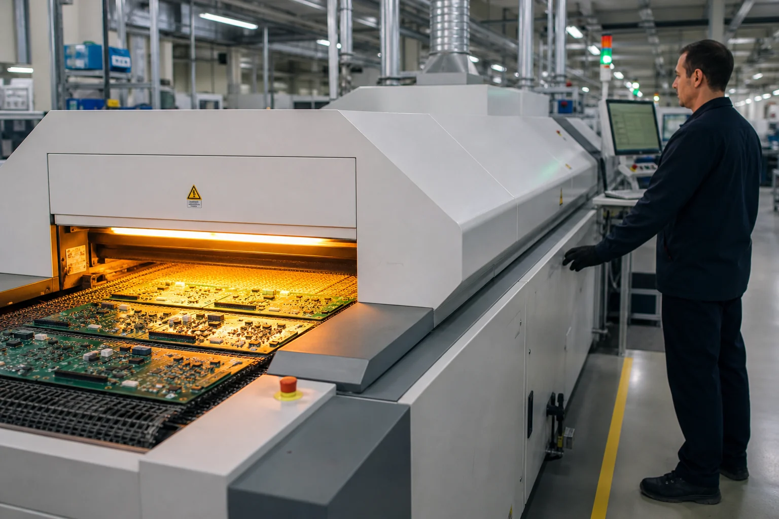
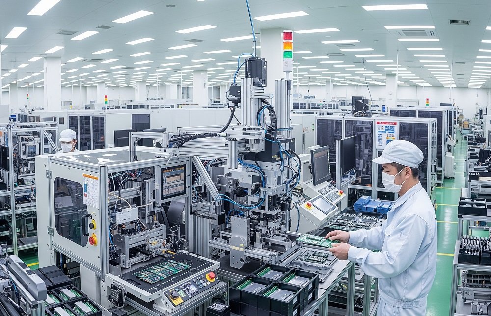
HDI PCB manufacturing process
The materials for HDI PCBs are very similar to what you’d find in conventional PCBs, but with higher concentrations of fillers such as silica and chopped fibers. It’s important to use materials that will withstand the high temperatures used in the board-building process. They are generally manufactured by the lamination method. The more the number of laminations, the higher the technology of the board. Ordinary HDI boards are basically one-time buildup, and high-end HDI uses two or more buildup technologies, while using advanced PCB technologies such as stacking, electroplating, and laser direct drilling.
The difficulty in HDI PCB fabrication lies in the fabrication of micro-vias, through metallization and fine lines.
Micro Via Fabrication
Microvia fabrication has always been a core issue for HDI PCB manufacturers. There are two main drilling methods:
- For common through hole drilling, mechanical drilling is always the best choice for its high efficiency and low cost. As machining capabilities have grown, so has its use in microvias.
- There are two types of laser drilling: photothermal ablation and photochemical ablation. The former refers to a process in which the operating material is heated to melt and evaporate through the formed through-holes after high-energy absorption of the laser light. The latter refers to the results of high-energy photons in the ultraviolet region and laser lengths exceeding 400 nm.
There are three types of laser systems applied to flexible and rigid boards, namely excimer laser, UV laser drilling, CO 2 laser. Laser technology is not only suitable for drilling, but also for cutting and forming. Even some manufacturers make HDI by laser. Although the cost of laser drilling equipment is high, they have higher precision, stable process and mature technology. The advantages of laser technology make it the most common method for blind/buried via fabrication. Today, 99% of HDI microvias are obtained by laser drilling.
Metallization
he biggest difficulty with through hole metallization is that the plating is difficult to achieve uniformity. For the deep-hole electroplating technology of micro-through holes, in addition to using the electroplating solution with high dispersing ability, the plating solution on the electroplating device should also be upgraded in time, which can be achieved by strong mechanical stirring or vibration, ultrasonic stirring, and horizontal spraying. In addition, the humidity of the through-hole walls must be increased prior to electroplating.
In addition to process improvements, HDI’s through-hole metallization methods have also seen improvements in major technologies: electroless additive technology, direct plating technology, and more.
Thin Lines
Thin line implementations include conventional image transfer and laser direct imaging. Traditional image transfer is the same process as ordinary chemical etching to form lines.
For laser direct imaging, photographic film is not required, and the image is formed directly on the photosensitive film by the laser. UV wave lamps are used for operation, enabling liquid corrosion protection solutions to meet the demands of high resolution and simple operation. Photographic film is not required to avoid adverse effects due to film defects, and can be directly connected to CAD/CAM, shortening the manufacturing cycle, making it suitable for limited and multiple productions.
Conclusion
High-density interconnect boards are a specialized type of printed circuit board designed for high-frequency and high-density connections. These boards are especially useful in high-power applications. They are made from thicker copper traces, a wider ground plane, and a higher-concentration fiberglass material that can withstand higher temperatures. However, these boards are not a good choice for low-frequency applications or circuits that require extensive wiring. The extra effort and expense to produce HDI boards are worth it for high-frequency and high-density applications that require a stiffer, more reliable circuit.