What is Gerber in PCB?
Gerber is a file format that has been used to share data between PCB manufacturers and suppliers since the 1980s. It was developed by Gerber Systems, Inc., a company that also produced the first CNC machine used for PCB fabrication. The term “Gerber” refers to graphic response bar encoding reference, which is an ASCII-based file format for documenting printed circuit board manufacturing data.
A non-digital file of a printed circuit board contains a lot of information about its design features as well as its fabrication requirements and other relevant details. Each printed circuit board has multiple layers and each layer has specific information about it—its type, copper thickness, drill data, component designs, locations of holes or vias (through holes), etc.
Contact Us For Gerber File Creation
Professional Quality Results. 24/7 Support
Why do we need Gerber Files for PCB Manufacturing?
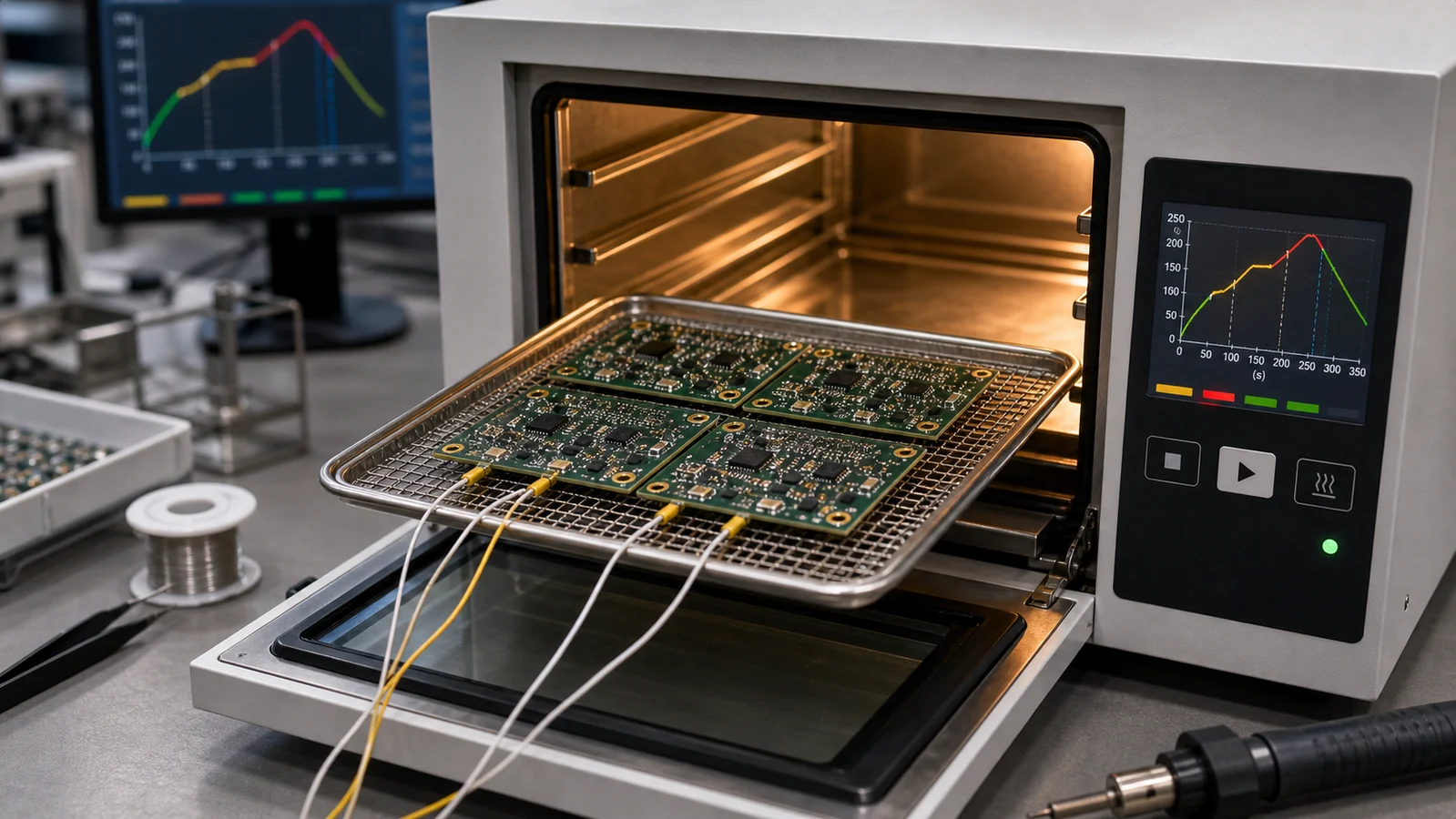
A printed circuit board design is created using computer-aided design (CAD) software. The CAD software is used to create a layout of the PCB and a list of components to be placed on it. This layout and components list is then exported as a layout file in either the Gerber or the Extended format. This file must then be sent to a PCB manufacturer to produce the PCB. The layout file in the Gerber format is sent to a PCB manufacturer and is later used to produce the PCB by fabricating the layer stack, etching the copper, plating the circuit board, drilling the holes, and soldering components on the PCB.
Types of Gerber Files for PCB
There are four different types of Gerber files for PCB manufacturing:
– Extended file: An Extended file is the most common file format for PCB data. It is an ASCII format and can be read by any CAD software or PCB manufacturer.
– Standard Gerber file: Standard Gerber files can show additional information like the thickness of the copper layers and the total thickness of the stack. Standard Gerber files can also be used to view the data in black and white.
– ILO file: An ILO file can be used to send the data of the layers in color. However, it can be read only by the software that created it.
– G-code file: A G-code file can be read only by the machine that created it. It can only be created using CAM software.
An example of a Gerber file in ASCII format:
					G04 Film Name:paste_top*
G04 Origin Date:Thu Sep 20 15:54:22 2007*
G04 Layer:PIN/PASTEMASK_TOP*
%FSLAX26Y26*MOIN*%
%IPPOS*%
%ADD28R,.11X.043*%
%ADD39O,.07X.022*%
%AMACRO19*
21,1,.0512,.0512,0.0,0.0,45.*%
%ADD19MACRO19*%
%LPD*%
G75*
D10*
X1762513Y1175000D03*
Y1374634D03*
Y1637506D03*
D39*
X4962513Y1425000D02*
Y1375000D01*
Y1325000D01*
Y1275000D01*
M02*
Functions of Gerber in PCB Manufacturing
The Gerber file is a machine-readable file that contains data about the circuit board design, such as the layer stack, copper thickness, drill data, component designs, locations of holes or vias, etc. The data is stored in a sequential form, which makes it easy for the machines to read and understand it. The machines use this information to fabricate the layers of the circuit board.
The data in the file can be read only when the PCB design is completely ready, i.e., when all the parts are soldered, the board has been etched, the board has been plated, etc. The data can then be used to produce the finished PCB design in the Extended format.
Limitations of Gerber in PCB Manufacturing
The main drawback of the Gerber file is that it cannot be edited or changed once it is created. If any changes need to be made to the PCB design, then a new file has to be created, sent to the PCB manufacturer, and then used to create the new PCB design.
Another drawback of the Gerber file is that it is not readable by humans. This means that if there is a problem with the data, it is difficult to know where the error is. Since the data is machine-readable, the error can be easily detected and corrected by machines. The data in the file must be correct, or there might be problems with the PCB design. For example, if the data does not specify the thickness of the layers or does not mention the type of finish, then the PCB fabrication may not be done correctly.
how to make PCB gerber files?
After the circuit board (PCB) design or reverse engineering is completed, designers need to hand over the relevant design files to the manufacturer for production. But sometimes for confidentiality or other reasons, we need to convert the PCB file into a gerber file, and then provide it to the manufacturer for production.
An example of how to convert pcb file to gerber file using Aulitum Designer 20:
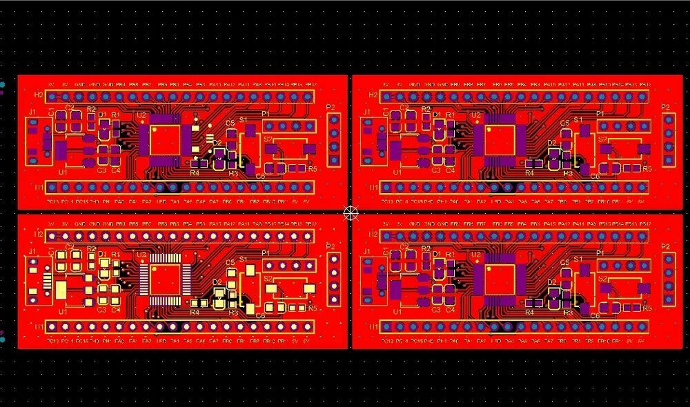
As shown in the figure below, the 2D view and 3D view of the pcb file that need to generate gerber are respectively.


In order for the manufacturer to get a complete PCB board information file, we need to go through 4 steps to set:
1. output gerber file
2. output Drilling file
3. output IPC net mark
4. output patch coordinate file
Finally, package all the files output in these 4 steps and send them to the manufacturer for production, and you are done!
The 4 specific steps are described below:
1. output gerber file
In the PCB interactive interface, execute the command “File-Fabrication Outputs-Gerber Files”, as shown in the following figure:

After executing this command, the gerber setting interface will pop up. There are 5 columns in this interface that need to be set.
(1) The settings of the “General” column are as shown in the figure below:

(2) The “Layers” column is set as shown in the figure below. It should be noted that “Plot Layers” should be selected as UsedOn, “MirrorLayers” should be selected as All Off, and “Include Unconnected mid-layer pads” should also be checked.


(3) The “Drill Drawing” column is set as shown below, just check the upper and lower boxes on the left:

(4) The settings of the “Apertures” column are as shown in the figure below, keep the default:

After setting, click ok, and the gerber file will be generated in the folder where the PCB is located, as shown in the following figure:

2. output Drilling file
We also need to output the information of mounting holes and vias on the PCB. At this time, we need to output the drilling file. In the PCB interactive interface, execute the command “File-Fabrication Outputs-NC Drill Files”, as shown in the following figure:

The following figure shows the drilling parameter setting interface, keep the default, and click ok. Likewise, data files related to drilling are generated in the folder where the PCB is located.

3. output IPC net mark
When submitting the gerber file to the manufacturer and generating the IPC netlist for the manufacturer to verify, some conventional open circuit and short circuit problems can be checked to avoid some losses. In the PCB interactive interface, execute the command “File-Assembly Outputs-Test Point Report”, as shown in the following figure:

The output settings of the IPC netlist are shown in the figure below, click ok, and the related files are also generated in the folder where the PCB is located:

4. output patch coordinate file
After the board is completed, the components need to be welded and patched. At this point, we need to use the coordinate information of each component. AD usually outputs coordinate files in txt format. In the PCB interactive interface, execute the command “File-Assembly Outputs-Generate Pick and Place Files”, as shown in the following figure:

The output settings of the patch coordinate file are as shown in the figure below, and you can keep the default:

At this point, all gerber files have been output. You can package all the gerber files generated in the directory where the PCB is located and send them to the manufacturer for production.
Conclusion
The Gerber file is an ASCII-based file format for documenting printed circuit board manufacturing data. It is used to share data between PCB manufacturers and suppliers. The data in the file can be read only when the PCB design is completely ready, i.e., when all the parts are soldered, the board has been etched, the board has been plated, etc. The data can then be used to produce the finished PCB design in the Excellon format. The main drawback of the Gerber file is that it cannot be edited or changed once it is created. If any changes need to be made to the PCB design, then a new file has to be created, sent to the PCB manufacturer, and then used to create the new PCB design. Another drawback of the Gerber file is that it is not readable by humans.