CMOS, or Complementary Metal Oxide Semiconductor, is a crucial component in various electronic devices, particularly in computers. This article aims to provide a comprehensive understanding of CMOS, its history, functions, applications, and related concepts.
Introduction to CMOS
What is CMOS?
CMOS stands for Complementary Metal Oxide Semiconductor, a technology that utilizes pairs of p-type and n-type MOSFETs (Metal Oxide Semiconductor Field-Effect Transistors) for logic functions. This technology is widely used in the construction of integrated circuits (ICs), including microprocessors, microcontrollers, memory chips, and digital logic circuits.
Characteristics of CMOS Devices
Two significant characteristics of CMOS devices are high noise immunity and low static power consumption. Since one transistor of the MOSFET pair is always off, the series combination draws significant power only momentarily during switching between on and off states. As a result, CMOS devices generate less waste heat compared to other forms of logic, like NMOS logic or transistor-transistor logic (TTL). These characteristics enable CMOS to integrate a high density of logic functions on a chip, making it the dominant MOSFET fabrication process for very large-scale integration (VLSI) chips.
History of CMOS
Origins and Development
The concept of complementary symmetry was first introduced by George Sziklai in 1953. However, the CMOS process was conceived by Frank Wanlass at Fairchild Semiconductor and presented by Wanlass and Chih-Tang Sah at the International Solid-State Circuits Conference in 1963. Wanlass later filed a US patent for CMOS circuitry, which was granted in 1967.
Commercialization and Adoption
RCA commercialized the technology with the trademark “COS-MOS” in the late 1960s, forcing other manufacturers to find another name, leading to “CMOS” becoming the standard name for the technology by the early 1970s. CMOS overtook NMOS logic as the dominant MOSFET fabrication process for VLSI chips in the 1980s, also replacing earlier transistor-transistor logic (TTL) technology.
In the 1990s, more advanced process technologies such as STI and Salicide (metal silicide) were applied to CMOS process technology. With the continuous development of process technology, the feature size of CMOS devices was gradually reduced in proportion. The working speed of the CMOS process integrated circuit is continuously improved, and at the same time, a lower power supply voltage can be selected, and the performance of the CMOS process integrated circuit can already compete with the bipolar process integrated circuit.
In the 21st century, with the rapid development of CMOS process technology, the advantages of CMOS process integrated circuits have been highlighted, such as high integration, strong anti-interference ability, high speed, low static power consumption, wide The power supply voltage range and wide output voltage range have made analog integrated circuit design technology advance by leaps and bounds. Due to the advantages of CMOS process technology in many aspects, it has become the preferred technology for digital circuits, analog circuits and digital-analog hybrid circuits. As of 2011, 99% of IC chips, including most digital, analog, and mixed-signal ICs, were fabricated using CMOS technology.
CMOS Process
CMOS is to manufacture NMOS and PMOS on the same chip to form an integrated circuit. CMOS process technology uses complementary symmetrical circuits to configure and connect PMOS and NMOS to form a logic circuit. The static power consumption of this circuit is almost zero. This theory can Solving the power consumption problem well, this discovery has laid a theoretical foundation for the development of CMOS process technology.
CMOS Inverter Circuit
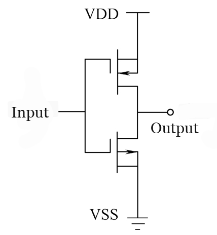
The figure below shows a CMOS inverter circuit composed of PMOS and NMOS, only when the input port changes from low level (VSS) to high level (VDD) or from high level (VDD) to low level (VSS) At the moment of transition, NMOS and PMOS will be turned on at the same time, and a current will be generated between VDD and VSS, thereby generating power consumption. When the input port is low level, only the PMOS is turned on, and when the input port is high level, only the NMOS is turned on, and no current will be generated between VDD and VSS, so the static power consumption is zero.

CMOS latch structure
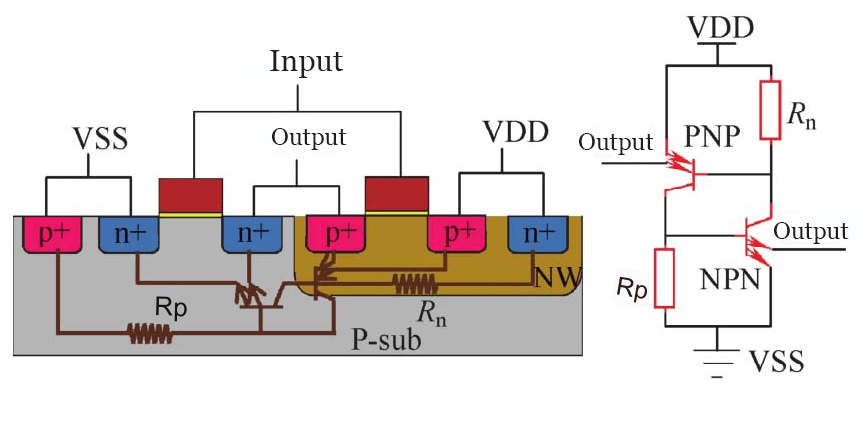
The following figure shows the parasitic PNPN latch structure in the CMOS inverter circuit. When there is noise at the output port, it will cause the parasitic bipolar transistor PNP or NPN to conduct, and then form a conduction current to flow through the resistor Rp or Rn Positive feedback is formed, causing another parasitic bipolar transistor to be turned on, and at this time, the two parasitic bipolar transistors are turned on at the same time to form a latch-up low-impedance path, which burns the chip. The advantages of CMOS process technology are small power dissipation and large noise tolerance, so early CMOS process technology is mainly used in electronic fields such as toys, watches and calculators that can tolerate slower speeds.

CMOS in Computers
CMOS Memory
In computers, CMOS refers to a small amount of memory on the motherboard that stores BIOS (Basic Input Output System) settings. This memory contains essential information, including the system time and date, as well as hardware settings.
CMOS Battery
The CMOS memory is powered by a battery, typically a coin-sized CR2032 cell, which provides constant power to the chip. This battery ensures that the CMOS retains its data even when the computer is turned off. A CMOS battery generally lasts around 10 years but may need to be replaced depending on the usage and environment of the computer.
Clearing CMOS
Clearing CMOS involves resetting the BIOS settings to their default levels, which can be a helpful troubleshooting step for various computer issues. This process is often necessary if the computer experiences freezing, hardware-related error messages, or CMOS battery failure.
CMOS Applications
Analog Circuits
CMOS technology is also used in analog circuits such as image sensors, data converters, RF (radio frequency) circuits, and highly integrated transceivers for various types of communication.
CMOS Image Sensors
A CMOS image sensor is a type of image sensor used in digital cameras to convert images into digital data.
Microprocessors and Microcontrollers
CMOS technology is employed in the development of microprocessors and microcontrollers, which are essential components of various electronic devices.
CMOS vs. BIOS
While CMOS and BIOS are closely related, they serve different functions within a computer. The BIOS is a computer chip on the motherboard responsible for communication between the processor and other hardware components. In contrast, CMOS is a RAM chip on the motherboard that stores the BIOS settings.
Check the following table for more details:
| Feature | CMOS | BIOS |
|---|---|---|
| Full Form | Complementary Metal-Oxide-Semiconductor | Basic Input/Output System |
| Function | Provides storage for system configuration data and real-time clock settings | Manages the initial hardware initialization process and provides a basic set of low-level routines |
| Nature | Memory technology | Software |
| Storage | Non-volatile memory | Flash memory or EEPROM (Electrically Erasable Programmable Read-Only Memory) |
| Purpose | Stores BIOS settings | Executes the BIOS firmware |
| Accessibility | Accessible during system operation | Accessible during system startup |
| Configuration Data | Holds system settings (e.g., date, time, boot order) | Contains firmware settings and parameters |
| Volatility | Retains data even when the system is powered off | Data can be modified or erased |
| Battery Backup | Requires a CMOS battery to retain data | Not applicable |
| Size | Small in size and capacity | Larger in size and capacity |


