What is Dual Inline Package?
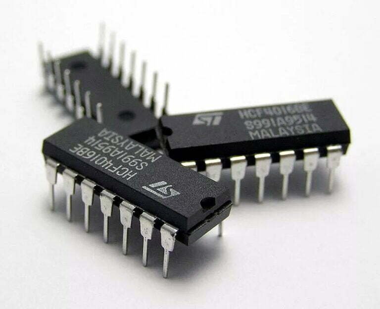
DIP, or dual inline package, is a type of integrated circuit (IC) packaging that features two parallel rows of metal pins, called dual in-line pins, on either side of a rectangular-shaped circuit. DIP packages can be soldered onto a printed circuit board or inserted into a DIP socket. DIP chips have two rows of pins and require insertion into a DIP socket on a chip carrier or can be directly soldered onto a printed circuit board. DIP packages have been widely used for ICs, DIP switches, LEDs, seven-segment displays, bar graph displays, and relays.
Types of Dual Inline Packages
- Ceramic DIP (CDIP): better electrical performance and higher resistance to heat, moisture, and shock.
- Plastic DIP (PDIP): consists of two parallel rows of pins, provides insulation and protection for the ICs.
- Shrink Plastic DIP (SPDIP): features with a small lead pitch 0.07 in (1.778mm).
- Skinny DIP (SDIP): comes with a width of 7.62mm and a pin center distance of 2.54mm.
History of DIP Package
Invention of DIP
The first DIP component was invented by Bryant Buck Rogers of Fairchild Semiconductor in 1964. It had 14 pins and was quite similar to today’s DIP packaging. The rectangular shape of DIP components increased the density of components on circuit boards compared to earlier round components. DIP components were also suitable for automated assembly equipment, with dozens to hundreds of ICs on a circuit board soldered by wave soldering machines and tested by automated testing equipment, requiring only a small amount of manual labor. The size of DIP components is actually much larger than the integrated circuits inside them.
From DIP to SMT
DIP packaging was the mainstream of the microelectronics industry in the 1970s and 1980s. Its usage gradually decreased in the early 21st century and was replaced by surface mount technology (SMT) packaging such as PLCC and SOIC. The characteristics of SMT components are suitable for mass production, but less convenient for circuit prototype production. As some new components only provide SMT packaging products, many companies produce adapters that convert SMD components to DIP packaging, allowing SMT ICs to be placed in the adapter and connected to breadboards or other direct-insertion components in a circuit prototype board (such as a punch plate) just like DIP components.
The Decline of DIP Components
For programmable components such as EPROM or GAL, DIP-packaged components are still popular for a while because they are convenient to burn data by external burning equipment (DIP packaged components can be directly inserted into the corresponding DIP socket of the burning equipment). . However, with the popularity of in-line programming (ISP) technology, the benefits of easy programming of DIP package components are no longer important. In the 1990s, components with more than 20 pins may still have DIP packaged products. In the 21st century, many new programmable components are packaged in SMT, and products in DIP package are no longer available.
DIP Structure
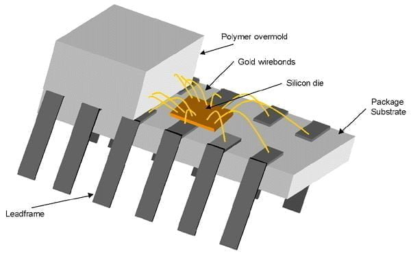
The DIP package consists of a leadframe, a package substrate, a silicon die, gold wirebonds, and a polymer overmold.

The leadframe is a thin metal frame that holds the silicon die and provides electrical connections to the outside world. The package substrate is a thin piece of insulating material that supports and electrically connects the leadframe and the silicon die.
The silicon die is the heart of the DIP package, containing the electronic circuitry that performs the desired function. The gold wirebonds connect the silicon die to the leadframe, allowing electrical signals to flow between the silicon die and the outside world.
The polymer overmold is a protective coating that covers the leadframe, package substrate, silicon die, and gold wirebonds. It provides mechanical protection, prevents moisture ingress, and improves the overall reliability of the DIP package.
Pros and Cons of Dual Inline Package
Pros
- Simple and low cost.
- Easy to manufacture and assemble for mass production.
- Compatible with through-hole mounting techniques.
- Good heat dissipation.
- Easy to replace without damaging the surrounding components.
Cons
- DIPs take up more space on the circuit board compared to other packaging types like SMT.
- They are not suitable for high-density applications, since their pin spacing is limited.
- DIPs are not as rugged as other packaging types and can be damaged by mechanical stress, such as bending or twisting.
- They can also be affected by temperature fluctuations, which can cause the pins to expand or contract and potentially lead to solder joint failure.
Pins of DIP
DIP (dual in-line package) components have standard dimensions that comply with JEDEC standards. The distance between two pins (pitch) is 0.1 inches (2.54 mm). The row spacing, which refers to the distance between two rows of pins, depends on the number of pins in the package. The most common row spacings are 0.3 inches (7.62 mm) or 0.6 inches (15.24 mm). Other less common spacings are 0.4 inches (10.16 mm) or 0.9 inches (22.86 mm). There are also some packages with a pitch of 0.07 inches (1.778 mm) and row spacings of 0.3 inches, 0.6 inches, or 0.75 inches.
DIP packages used in the former Soviet Union and Eastern Europe are similar to JEDEC standards, but the pitch is 2.5 millimeters, which is based on the metric system, rather than 0.1 inches (2.54 mm) used in the imperial system.
The number of pins in a DIP package is always even. If the row spacing is 0.3 inches, the most common number of pins is from 8 to 24, and sometimes there are packages with 4 or 28 pins. If the row spacing is 0.6 inches, the most common numbers of pins are 24, 28, 32, or 40, and there are also packages with 36, 48, or 52 pins. The maximum number of pins for commonly used DIP packages is 64, as in the case of the Motorola 68000 and Zilog Z180 CPUs.
When the identifying notch of a component is facing up, the upper-left pin is pin 1, and the other pins are numbered counterclockwise. Sometimes pin 1 is also marked with a dot. For example, in a DIP14 IC, when the identifying notch is facing up, the pins on the left side are numbered from 1 to 7 from top to bottom, and the pins on the right side are numbered from 8 to 14 from bottom to top.
Electrical Characteristics of DIP Components
DIP (dual in-line package) components have specific electrical characteristics that determine their performance and reliability. The following are some of the most important electrical specifications for DIP components:
- Electrical Life: Each switch is tested for 2000 cycles at 24VDC and 25mA.
- Rated Current for Infrequent Switching: 100mA, withstand voltage of 50VDC.
- Rated Current for Frequent Switching: 25mA, withstand voltage of 24VDC.
- Contact Resistance: (a) Maximum initial value of 50mΩ; (b) maximum value after testing of 100mΩ.
- Insulation Resistance: Minimum of 100mΩ at 500VDC.
- Withstand Voltage: 500VAC/1 minute.
- Inter-electrode Capacitance: Maximum of 5pF.
- Circuit: Single-pole, single-throw (SPST) or double-pole, double-throw (DPDT) configurations are available.
These electrical characteristics are crucial for ensuring the optimal performance and reliability of DIP components. Manufacturers must adhere to the JEDEC standards to ensure that their components meet the required specifications. When designing circuits that use DIP components, it is important to consider these electrical characteristics to ensure that the circuit functions properly and safely.
DIP vs SOIC
DIP (dual in-line package) and SOIC (small outline integrated circuit) are two commonly used packaging types for integrated circuits (ICs). Both types have their advantages and disadvantages, and the choice between them depends on the specific requirements of the application. The following table summarizes the main differences between DIP and SOIC.
| Feature | DIP | SOIC |
|---|---|---|
| Pin Count | Up to 64 pins | Up to 48 pins |
| Pitch | 0.1 inches (2.54 mm) | 0.5 mm to 1.27 mm |
| Size | Larger than SOIC | Smaller than DIP |
| Through-Hole Mounting | Yes | No |
| Surface Mounting | No | Yes |
| Lead Count | Even | Even or Odd |
| Lead Position | Inline | Gull-wing and J-lead |
| Electrical Performance | Good | Better than DIP |
| Cost | Lower than SOIC | Higher than DIP |
DIP packages have been widely used for many years, but their size and through-hole mounting make them less suitable for modern surface-mount technology (SMT) applications. SOIC packages, on the other hand, are smaller, lighter, and more suitable for SMT assembly. The lead position of SOIC packages also allows for better electrical performance, as the leads have shorter paths to the IC.
In terms of cost, DIP packages are generally less expensive than SOIC packages. However, the cost difference may be offset by the advantages of SOIC packages in terms of performance, size, and ease of assembly.
In summary, DIP packages are suitable for applications that require lower pin count and through-hole mounting, whereas SOIC packages are more suited for applications that require higher pin count, smaller size, and surface-mount technology.


