The first bipolar junction transistor was invented at Bell Laboratories in 1947. “Bipolar” is referred to as bipolar, hence the name bipolar junction transistor (BJT). A BJT is a three-terminal device with a collector (C), base (B) and emitter (E).
There are currently two types of bipolar junction crystals, namely NPN and PNP transistors. In this article, we will introduce the PNP transistor structure, working principle and application.
What is a PNP Transistor?
PNP transistor is a type of bipolar junction transistor (BJT) that consists of three layers of doped semiconductors. In a PNP transistor, the majority charge carriers are holes, which flow from the emitter to the base and then to the collector. The PNP transistor is widely used in electronic circuits as a switch or amplifier.
Structure of PNP Transistor
To illustrate the structure of a PNP transistor, consider the following diagram:

A PNP transistor consists of three layers of alternating P-type and N-type semiconductor materials. The three layers are called the emitter (E), base (B), and collector (C). The layers are arranged in a sandwich-like structure with two p-type layers surrounding an n-type layer, hence the name PNP.
In this diagram, the emitter is on the left, the collector is on the right, and the base is in the middle. The base is very thin and lightly doped, while the emitter and the collector are heavily doped. The doping of the layers creates junctions between them, which are responsible for the functioning of the transistor.
When a voltage is applied to the base of the PNP transistor, a small current flows from the emitter to the base. This current causes a much larger current to flow from the collector to the emitter, which can be used to control an external circuit.

How does PNP Transistor Work?
As mentioned above, a transistor is a current control device which has two depletion layers with a specific barrier potential required to diffuse the depletion layers. The barrier potential of a silicon transistor is 0.7V at 25°C, while that of a germanium transistor is 0.3V at 25°C. The most commonly used type of transistor is silicon because it is the most abundant element on Earth after oxygen.

Internal Operation:
The structure of a PNP transistor is that the collector and emitter regions are doped with p-type material, and the base region is doped with a small layer of n-type material. The emitter region is heavily doped compared to the collector region. These three regions form two junctions, which are the collector-base junction (CB) and the base-emitter junction.
When a negative potential VBE falling from 0V is applied across the base-emitter junction, electrons and holes begin to accumulate in the depletion region. When the potential is further lowered below 0.7V, the barrier voltage is reached and diffusion occurs. Therefore, electrons flow towards the positive pole, and the base current (IB) is opposite to the electron flow. Also, if a voltage VCE is applied at the collector terminal, a current starts flowing from the emitter to the collector. Therefore, PNP transistors can act as both switches and amplifiers.
Operating Area and Operating Mode:
- Active area: IC = βxIB – amplifier operation
- Saturation region: IC = saturation current – switching operation (fully on)
- Cut-off area: IC=0—switching operation (completely closed)
Application Examples of PNP transistors
1. PNP Transistor as Switch
PNP transistors are often used as switches in circuits. In this example we use PSPICE model and PN2907A transistor. First remember to use a current limiting resistor at the base. Higher base current can damage the BJT. According to the datasheet below, the maximum continuous collector current is 600mA and the corresponding gain (hFE or β) is given in the datasheet as a test condition. The corresponding saturation voltage and base current are also available.

Steps to select components:
1. Find the collector current, which is the current drawn by the load. In this case it would be 200mA (in parallel with LED or load) and resistance = 60 ohms.
2. In order to drive the transistor into a saturated state, enough base current must be drawn to make the transistor fully turned on. Calculate the base current and the corresponding resistor to use. The following is the calculation formula of base current and base resistance in PNP transistor:
IB=IC/β=-200 mA / 90=-2.2 mA≈-2.5mA
RB=VBE/IB=-5/-2.5 mA=2000 Ohm≈2.2k Ohm
For full saturation, the base current is about 2.5mA (not too high or too low). So below is the circuit for 12V to base, same as for emitter to ground, during which time the switch is off.

Theoretically, the switch is fully open, but in practice a leakage current can be observed. This current is negligible since their units are pA or nA. To better understand current control, a transistor can be thought of as a variable resistor across the collector (C) and emitter (E), whose resistance changes according to the current through the base (B).
Initially, when no current flows through the base, the resistance across CE is so high that no current flows through it. When a potential difference of 0.7V and above appears at the base terminal, the BE junction diffuses and causes the CB junction to diffuse. Now the current flowing from the emitter to the collector is proportional to the current flowing from the emitter to the base, which is the gain.
Now let’s see how to control the output current by controlling the base current. Fixed IC = 100mA, although the load is 200mA, the corresponding gain in the datasheet is between 100 and 300, and following the same formula above, we get:
IB=IC/β=-100 mA/250=-0.4 mA
RB=VBE/IB=-5/-0.4 mA=12500 Ohm≈13k Ohm
The difference between the actual and calculated values is due to the voltage drop across the transistor and the resistive load used. Also, the standard resistor value of 13k0hm was used at the base instead of 12.5kohm.
2. PNP Transistor as Amplifier
Amplification is the conversion of a weak signal into a usable form. The amplification process is an important step in many applications such as wirelessly transmitting signals, wirelessly receiving signals, Mp3 players, mobile phones, etc. Transistors can amplify power, voltage and current in different configurations.
Some configurations used in transistor amplifier circuits are:
- common emitter amplifier
- common collector amplifier
- common base amplifier
Among the above types, the common emitter type is the most commonly used configuration. This operation occurs in the active region, an example being a single-stage common-emitter amplifier circuit. A stable dc bias point and a stable ac gain are important for amplifier design. The name single-stage amplifier when only one transistor is used.

Above is a single-stage amplifier, where a weak signal applied at the base terminal is converted to beta times the actual signal at the collector terminal.

Amplifier Circuit Configurations of PNP Transistors
Amplifier circuits come in three configurations: common emitter (CE), common base (CB), and common collector (CC). These configurations use different capacitive and resistive elements for signal amplification and stabilization.
Common emitter (CE)
The CE (common emitter) configuration includes a coupling capacitor (CIN) and an output coupling capacitor (COUT). CIN couples the input signal to the base of the transistor, allowing AC signals to pass while isolating DC signals. COUT couples the output signal of the transistor to the load circuit and only allows the AC signal to pass through. The CE configuration also uses a bypass capacitor as a low resistance path for the amplified signal.

In the CE configuration, R2 and RE are used to provide amplifier stability, while R1 and R2 together act as a voltage divider to ensure stability at the DC bias point.
Common Base (CB)
In a CB amplifier, the input is applied to the emitter terminal, and the output is taken from the collector terminal. The emitter terminal is forward-biased, while the collector terminal is reverse-biased. The biasing conditions of a CB amplifier provide a low input impedance and a high output impedance.

The common base amplifier circuit can be represented by the following equation: Av = -gmRc, where Av is the voltage gain, gm is the transconductance parameter, and Rc is the load resistor. The voltage gain of a common base amplifier is less than one, but it has a high current gain and a wide bandwidth.
Common Collector (CC)
The CC amplifier is also known as an emitter follower because the output voltage follows the input voltage closely. In a CC amplifier circuit, the emitter terminal is always biased at a voltage slightly less than the base voltage, typically around 0.6V for a silicon transistor. This ensures that the transistor is in the active region and can amplify the input signal.

The CC amplifier has a high input impedance and a low output impedance, which makes it suitable for impedance matching and voltage amplification applications. It also offers high current gain and high unity-gain bandwidth, which makes it ideal for buffering signals between stages of an amplifier.
Engineering checks for PNP transistor switching circuits
Before using PNP transistor switching circuits in a PCB, firmware, repair, or validation workflow, confirm the details that usually decide whether the design works reliably instead of only reading the headline specification.
Design and troubleshooting checklist
| Area | What to check | Why it matters |
|---|---|---|
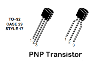
| Pinout and package | Confirm E-B-C order for TO-92, SOT-23, and manufacturer variants | A swapped emitter and collector causes low gain and heating |
| High-side switching | Calculate base resistor, load current, saturation voltage, and MCU drive polarity | PNP stages turn on when the base is pulled below the emitter |
| Protection | Check base-emitter reverse voltage, flyback path, and thermal dissipation | Inductive loads and wrong bias can damage the junction |
These checks help connect the search intent around PNP transistor pinout and applications with practical board-level decisions, component selection, and failure analysis.