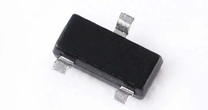
What is NMOS transistor?
An NMOS transistor is a type of field-effect transistor (FET) that operates using negative polarity.
NMOS Structure
It is made up of three regions: the source, the drain, and the gate. The source is where the current enters, the drain is where it exits, and the gate controls the flow of current. When a voltage is applied to the gate, it creates an electric field that influences the behavior of the electrons in the channel between the source and drain. This can either enhance or deplete the flow of current through the transistor.

Engineering checks for NMOS transistor operation and circuit checks
Before using NMOS transistor operation and circuit checks in a PCB, firmware, repair, or validation workflow, confirm the details that usually decide whether the design works reliably instead of only reading the headline specification.
Design and troubleshooting checklist
| Area | What to check | Why it matters |
|---|---|---|
| Gate drive | Check VGS threshold, required enhancement voltage, gate charge, and MCU drive strength | Threshold voltage is not the same as low RDS(on) operation |
| Switching path | Review source reference, body diode direction, load current, and flyback protection | Wrong NMOS orientation can bypass the intended switch |
| Thermal | Calculate conduction loss, switching loss, package rating, and copper heat spreading | Small MOSFET packages can overheat before reaching headline current |
These checks help connect the search intent around NMOS transistor with practical board-level decisions, component selection, and failure analysis.
How does NMOS Work?
NMOS operates by controlling the flow of current through a conductive channel between the source and drain terminals by applying an electric field to a gate electrode, which is separated from the channel by a thin insulating layer.
When the gate-to-source voltage (vGS) is zero, and even if the drain-to-source voltage (vDS) is applied, the PN junctions between the source and drain of an NMOS transistor are reverse-biased, and the depletion region between them becomes too wide to support the flow of current. Therefore, the current between the drain and source (iD) is negligible.
However, when vGS is positive, an electric field is generated in the SiO2 insulation layer between the gate and substrate. This field attracts electrons and repels holes from the substrate near the gate, creating a depletion region. When the magnitude of vGS increases, more electrons are attracted to the surface of the substrate, forming an N-type channel that connects the source and drain terminals. The channel is then able to support the flow of current between the source and drain terminals.
The voltage at which the channel just begins to form is called the threshold voltage (VT). An NMOS transistor is considered an enhancement-mode transistor because it requires vGS to be greater than VT to create a conductive channel.
The drain-to-source voltage (vDS) affects the current flowing through the channel. As vDS increases, the thickness of the channel near the drain decreases, and the current increases. However, when vDS reaches a value equal to vGS minus VT, the channel narrows to the point where the current no longer increases, and the transistor enters saturation mode.
In summary, an NMOS transistor operates by creating a conductive channel between the source and drain terminals when a positive voltage is applied to the gate, allowing current to flow between the source and drain terminals. The current is controlled by the voltage applied to the gate and drain terminals.
NMOS vs PMOS
NMOS and PMOS are both the Metal-Oxide-Semiconductor, there’re some difference between them:
| NMOS | PMOS | |
|---|---|---|
| Polarity | Negative | Positive |
| Channel type | n-type | p-type |
| Carrier type | Electrons | Majority holes |
| Threshold voltage | Positive | Negative |
| Switching speed | Fast | Slow |
| Cost | Cheap | Expensive |
| Power consumption | High | Low |
| Applications | Logic gates, memory cells, amplifiers | Level shifters, power management circuits, analog circuits |
Application of NMOS
NMOS transistors are commonly used in digital circuits as switches or amplifiers. They can also be found in microprocessors, memory chips, and other electronic devices.