What is TTL?
TTL, or Transistor-Transistor Logic, is a type of digital circuit design that uses bipolar transistor technology to create logic gates. TTL is commonly used in electronics, particularly in the design of digital circuits, because it is fast and reliable. It is also relatively easy to understand and design with TTL logic, making it a popular choice for hobbyists and professionals alike.
For example, a simple TTL logic circuit might be used to control the operation of a motor in a robotic arm. The TTL logic circuit would receive input from sensors that detect the position of the arm, and then use transistors to control the flow of current to the motor, causing it to move in the desired direction. This type of circuit can be designed using a TTL logic gate array, which is a collection of pre-designed TTL logic gates that can be combined to create more complex circuits.
How Does TTL Work?
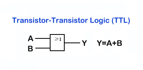
Transistor-Transistor Logic (TTL) is a popular digital logic family that uses bipolar junction transistors (BJTs) to implement various logic functions. TTL operates based on the concept of switching between two voltage levels, typically referred to as “high” and “low” or “1” and “0” states.
The basic building block of TTL is the transistor, which is used as a switch. In TTL, there are two types of logic gates: NAND gates and NOR gates. These gates are formed by connecting multiple transistors in a specific arrangement.
Let’s take a simple example of a TTL NAND gate to understand how TTL works. A NAND gate has multiple inputs and a single output. The output of the NAND gate is high (logic 1) only when all of its inputs are low (logic 0). Otherwise, the output is low (logic 0).
In TTL, a NAND gate is implemented using transistors. Specifically, it uses multiple transistors in a configuration known as a transistor network. The specific arrangement of the transistors allows the gate to perform the desired logic function.
Here’s a simplified representation of a TTL NAND gate:

In this representation, A and B are the inputs, and the Output is the resulting output. Each input (A and B) is connected to the base of a transistor. The emitters of the transistors are connected to ground (0V), and the collector of each transistor is connected to the output.
When the inputs A and B are both at logic 1 (high), a current flows through the base-emitter junction of the transistors, turning them on. This creates a low resistance path from the collector to the emitter, effectively connecting the output to ground (logic 0).
Conversely, if either input A or B (or both) is at logic 0 (low), no current flows through the base-emitter junctions of the transistors, keeping them off. This prevents the output from being connected to ground and allows it to remain at logic 1 (high).
Therefore, the output of the NAND gate is high (logic 1) only when all inputs are low (logic 0). Otherwise, the output is low (logic 0).
TTL gates are typically interconnected to create more complex digital circuits, such as adders, multiplexers, and flip-flops, enabling the implementation of various computational tasks in electronic systems.
It’s important to note that while TTL was widely used in the past, it has been largely replaced by other logic families, such as CMOS (Complementary Metal-Oxide-Semiconductor), which offer advantages in terms of power consumption and integration density.
How to Use TTL Circuit?
There are different types of TTL as follows:
- Standard TTL circuit
- Fast TTL circuit
- Schottky TTL circuit
- High Power TTL Circuit
- Low power consumption TTL circuit
- Advanced Schottky TTL circuit
Standard TTL circuit
The diagram below shows the internal structure and characteristics of a standard TTL NAND gate. Its NAND gate is a four-way two-input type. There are four 5400/740 circuits. In simple terms, this type of TTL circuit works as follows.

Q1 shown in the diagram is a dual emitter NPN transistor, this type of NAND gate is similar to two transistors with their base and emitter terminals connected together. Diodes named D2 and D3 are used to limit the input voltage which is negative in nature.
Low power TTL circuit
Low power TTL circuitry achieves low power consumption and dissipation. Although the speed at which operations are completed is reduced. The picture above is a low-power TTL made using AND gates. The NAND gate used here is a 74L00 or 54L00 type, the structure of this type of TTL is almost similar to that of standard TTL, except that the resistance value is higher. For this increased resistance value, the power dissipation of the circuit is reduced.

High power TTL circuit
Unlike low-power TTL, high-power TTL is a high-speed version of standard TTL. This type of TTL runs faster than previously discussed. It consumes more power than the other TTLs discussed previously. The figure below is a high power TTL NAND gate. NAND gates are quadruple two-input 74H00 or 54H00 types. Very similar to standard TTL except the Q3 transistor and D1 diode combination has been replaced by an arrangement of Q3, Q5 and R5. This type of TTL runs at a higher speed and consumes more power.

Schottky TTL circuit
A Schottky TTL circuit is used to speed up the operation time. This type of TTL provides twice the speed of high-power TTL. The power consumption is the same for both TTLs, no extra power consumption. The figure below represents a basic NAND based Schottky TTL diagram.
The circuit diagram is very similar to the high power TTL, the Q transistor of the high power TTL is missing here. The Schottky transistor used for this type of TTL is a bipolar transistor whose base and collector are connected by a Schottky diode.

Pros and Cons of TTL
Pros:
– TTL logic is simple and easy to understand.
– It has a fast switching speed due to low propagation delay.
– TTL can operate at a wide range of temperatures and voltages.
– It provides noise immunity due to the use of complementary transistors.
– It has a low power consumption compared to other logic families.
– TTL can be easily interfaced with other logic families.
Cons:
– The power consumption increases with an increase in the number of gates connected.
– The output voltage levels are limited, typically between 0 and 5 volts.
– TTL gates are not very efficient when driving capacitive loads.
– The output current is limited, which can be a problem when driving some loads.
– It requires a higher voltage supply compared to other logic families, which can lead to heat dissipation issues.
– TTL is not suitable for high-speed applications where very low propagation delays are required.
Engineering checks for TTL logic gates and board-level interface checks
Before using TTL logic gates and board-level interface checks in a PCB, firmware, repair, or validation workflow, confirm the details that usually decide whether the design works reliably instead of only reading the headline specification.
Design and troubleshooting checklist
| Area | What to check | Why it matters |
|---|---|---|
| Logic levels | Check VIH, VIL, VOH, VOL, fan-out, and current sink/source requirements | TTL inputs and CMOS inputs do not always share the same margins |
| Unused inputs | Tie unused inputs to a defined state through proper logic or resistors | Floating TTL inputs increase current and create intermittent switching |
| Timing | Review propagation delay, setup/hold paths, and power decoupling near each IC | Old logic families can still cause timing faults on simple boards |
These checks help connect the search intent around TTL logic with practical board-level decisions, component selection, and failure analysis.