| No. | Characteristics | BJT | MOSFET |
|---|---|---|---|
| 1 | Transistor Type | Bipolar Junction Transistor | Metal Oxide Semiconductor Field-Effect Transistor |
| 2 | Classification | NPN BJT and PNP BJT | P-channel MOSFET and N-channel MOSFET |
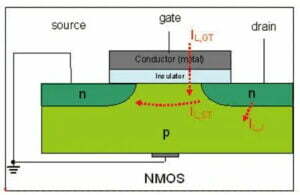
| 3 | Port | Base, Emitter, Collector | Gate, Source, Drain |
| 4 | Symbol |  |  |
| 5 | Charge Carrier | Both electrons and holes serve as charge carriers in BJT | Either electrons or holes serve as charge carriers in MOSFET |
| 6 | Control Mode | current-controlled | oltage-controlled |
| 7 | Input Current | milliamps/microamps | picoamps |
| 8 | Switching Speed | BJT is lower: maximum switching speed is close to 100KHz | MOSFET is higher: maximum switching frequency is 300KHz |
| 9 | Input Impedance | low | high |
| 10 | Output Impedance | low | medium |
| 11 | Temperature Coefficient | BJT has a negative temperature coefficient and cannot be connected in parallel | MOSFET has a positive temperature coefficient and can be connected in parallel |
| 12 | Power Consumption | high | low |
| 13 | Frequency Response | poor | good |
| 14 | Current Gain | BJT has low and unstable current gain: the gain can decrease once the collector current increases. If the temperature increases, the gain can also increase | MOSFET has high current gain and is almost stable for changing drain current |
| 15 | Secondary breakdown | BJT has a second breakdown limit | MOSFET has a safe operating area similar to BJT but does not have a second breakdown limit |
| 16 | Static Electricity | Static discharge is not a problem in BJT | Static discharge can be a problem in MOSFET and can lead to other issues |
| 17 | Cost | cheaper | more expensive |
| 18 | Application | low-current applications such as amplifiers, oscillators, and constant current circuits | high-current applications such as power supplies and low-voltage high-frequency applications |