What Does PMOS Mean?
PMOS (P-channel Metal-Oxide-Semiconductor) transistor is a type of field-effect transistor (FET) that is commonly used in electronic circuits.
PMOS Symbol
The PMOS symbol is a circle with an arrow pointing inward. The circle represents the p-type substrate and the arrow inside shows the direction of the majority carriers, which are holes.
The terminals are labeled as “G” for gate, “D” for drain, and “S” for source. Both the drain and source terminals are p-type doped regions. The gate terminal is a metal electrode separated from the substrate by a thin oxide layer. Applying a voltage to the gate creates an electric field in the oxide layer, controlling the majority carrier flow between the drain and source.

How Does a PMOS Transistor Work?
A PMOS operates based on the same principle as an NMOS transistor, but with a different doping profile.
In a PMOS transistor, the substrate is made of n-type silicon, and the source and drain regions are made of p-type silicon. The gate is separated from the substrate by a layer of oxide (usually silicon dioxide) and is connected to a positive voltage supply. When a negative voltage is applied to the gate, a depletion region is formed between the p-type source and drain regions, which prevents the flow of current.

However, when a positive voltage is applied to the gate, it attracts holes (the majority carriers in p-type silicon) to the interface between the source and drain regions, creating a conductive channel for current to flow. The channel resistance is proportional to the gate-to-source voltage (VGS), so as VGS becomes more positive, the channel resistance decreases, allowing more current to flow.
When the VGS exceeds a certain threshold voltage (VTP), the channel becomes fully depleted, and the transistor enters the saturation region, where the drain current is nearly independent of the drain-to-source voltage (VDS). In the triode region, where VDS is small, the transistor behaves like a variable resistor whose resistance is proportional to VGS.
PMOS transistors are commonly used in complementary metal-oxide-semiconductor (CMOS) circuits, where they are paired with NMOS transistors to form logic gates and other digital circuits.
PMOS vs NMOS
| PMOS | NMOS | |
|---|---|---|
| Symbol | Circle with an arrow pointing inward | Circle with an arrow pointing outward |
| Substrate | p-type | n-type |
| Majority carrier | Holes | Electrons |
| Gate voltage polarity | Negative | Positive |
| Electric field direction in oxide layer | Towards the substrate | Away from the substrate |
| Threshold voltage | Positive | Negative |
| Switching speed | Slow | Fast |
| Power consumption | Low in steady state | High in steady state |
| Applications | Low-power circuits | High-performance circuits |
Engineering checks for PMOS Transistors: How They Work & Applications
Before using PMOS Transistors: How They Work & Applications in a PCB, firmware, repair, or validation workflow, confirm the details that usually decide whether the design works reliably instead of only reading the headline specification.
Design and troubleshooting checklist
| Area | What to check | Why it matters |
|---|---|---|
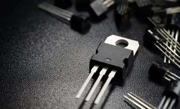
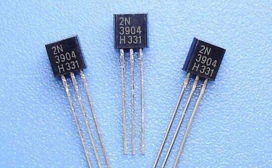
| Pinout and package | Verify the diagram of pmos pinout, package variant, polarity, and footprint before assembly | Similar packages can have different pin order or exposed-pad rules |
| Electrical limits | Check voltage, current, power, frequency, thermal rating, and derating | Headline ratings rarely apply in every PCB condition |
| Substitution | Compare datasheets, markings, tolerances, and circuit role before replacing parts | Equivalent parts still need board-level evidence |
These checks help connect the search intent around diagram of pmos with practical board-level decisions, component selection, and failure analysis.