Dual inline package meaning sounds simple at first: an integrated circuit package with two parallel rows of leads. But on a real PCB, that package style also implies through-hole assembly, larger board area, easier socketing, easier hand replacement, and a very different manufacturing tradeoff from modern fine-pitch surface-mount parts.
That is why engineers still care about DIPs long after denser packages took over most production electronics. A DIP is rarely the smallest or cheapest answer per square millimeter, yet it can still be the practical answer when prototyping speed, service access, connector-like durability, or socketed replacement matters more than compactness.
What a Dual Inline Package Actually Is
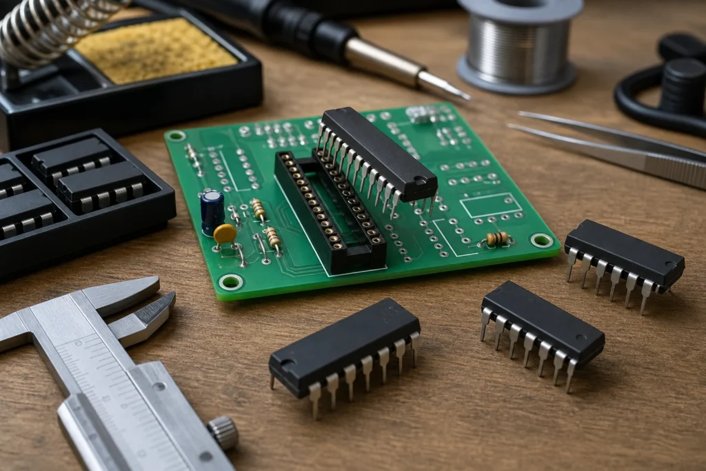
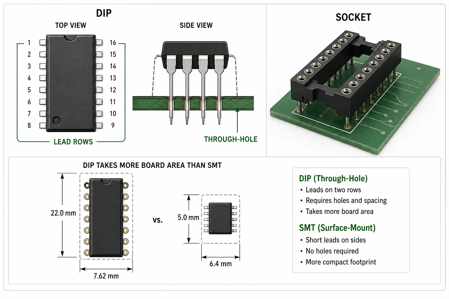
A dual inline package, usually shortened to DIP, places the IC body between two rows of leads that insert into plated through-holes on the PCB or into a compatible socket. The form factor became popular because it is easy to handle, easy to inspect, and mechanically straightforward for both manual assembly and automated insertion.
In practical terms, a DIP usually tells you a few things before you even read the datasheet:
The part expects through-hole mounting rather than direct SMT pads.
Lead spacing and body width are generous compared with modern leaded or leadless SMD packages.
Socketing is often possible, which changes service and prototyping options.
Board area consumption will usually be higher than an SMT alternative with the same function.
Why DIPs Still Show Up on Real Projects
DIP packages survive because they solve practical problems that smaller packages do not solve as well.
Prototype convenience. A DIP is easy to breadboard, socket, hand solder, and swap during early debug.
Repairability. In field-serviceable products or lab equipment, replacing a socketed DIP is far less invasive than reworking a dense QFN or BGA.
Educational visibility. Pin spacing is wide enough for learners and technicians to trace signals, probe pins, and understand the circuit without magnification-heavy work.
Mechanical tolerance. Through-hole anchoring can be useful when the part will see repeated insertion cycles or rough handling during development.
Where the DIP Package Becomes a Liability
DIP convenience comes with costs, and they show up quickly in production-focused boards.
Board density drops. Through-holes consume routing area on multiple layers and force more generous placement clearances.
Assembly cost rises. Through-hole insertion, soldering, and inspection generally cost more than straightforward SMT placement at scale.
Profile height increases. Tall bodies and sockets create enclosure and vibration considerations that small SMDs often avoid.
Mixed-technology flow gets harder. If the board is mostly SMT, even one DIP may require selective soldering, hand soldering, or a secondary process step.
Those tradeoffs are why many designs move from DIP during development to surface-mount packages in production. The electrical function may stay the same while the manufacturing window changes completely.
What DIP Means for PCB Layout and Assembly
If you choose a DIP footprint, the package affects more than hole placement. Designers should still think about annular ring robustness, drill tolerance, wave or hand-solder access, adjacent tall parts, and whether a socket will be used in the finished build.
Assembly engineers care about different details: lead forming consistency, insertion alignment, barrel fill, solder-side access, and whether thermal mass around the holes makes hand soldering inconsistent. A DIP can be forgiving compared with fine-pitch SMT, but it is not immune to bad process control. Poor hole sizing or weak wetting can still create intermittent joints that only show up later in vibration or rework.
That also explains why through-hole versus surface-mount decisions, wave soldering process fit, and through-hole soldering technique still matter when a design includes even a small number of DIP parts.
When a DIP Is Still the Better Choice
A DIP is usually still defensible when the board is low volume, intended for socketed IC replacement, used in training or lab settings, or needs generous hand-access during debug. It can also make sense when the rest of the design is already through-hole and the manufacturing flow is built around that assumption.
It is much harder to justify when the product is space-constrained, high-volume, or already optimized for SMT line throughput. In that environment, DIP usually means extra board area, extra labor, and extra exceptions in the process traveler.
The Meaning of DIP Is Really About Package Tradeoffs
The literal dual inline package meaning is easy to state. The useful engineering meaning is broader: you are choosing a package that favors access, socketing, and visibility over density and high-volume assembly efficiency. Once that tradeoff is clear, it becomes easier to decide whether a DIP belongs on the final board or only on the prototype bench.
FAQ
What does dual inline package mean?
It refers to an IC package with two parallel rows of leads, typically intended for through-hole insertion into a PCB or socket.
Why are DIP packages still used if SMT packages are smaller?
DIPs are still useful for prototypes, socketed devices, educational boards, and serviceable products because they are easier to handle, inspect, replace, and probe.
Is a DIP package better for repair work?
Often yes, especially when the part is socketed or when the board allows clear solder-side access. Repair effort is usually lower than with dense leadless SMT packages.
What is the main downside of a DIP on a modern PCB?
The biggest downside is usually board area and process cost. Through-holes reduce routing freedom, and mixed SMT plus DIP assembly often adds secondary soldering or inspection steps.