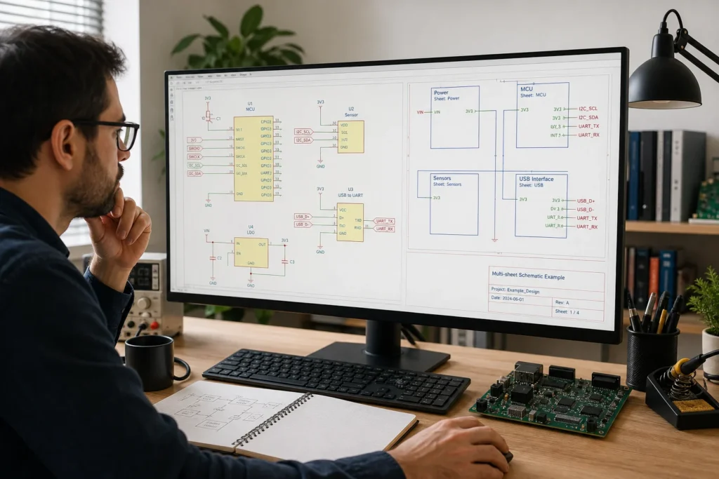
In KiCad, labels are not decoration. They decide whether a net stays local to one sheet, jumps across the whole project, or passes through a hierarchy in a controlled way. If you label too casually, the schematic may still look tidy while the connectivity becomes harder to review than a page full of wires.
That is why the real question behind how to make labels in KiCad is not just where to click. It is how to name nets so another engineer can tell, at a glance, which signals are intentionally shared, which ones belong only inside a block, and which ones should never have been made global in the first place.
Start With the Label Type, Not the Text
KiCad gives you several ways to label a net, and they do different jobs:
Local labels name a net inside the current sheet. They are the safest default when the signal does not need to leave that page.
Global labels connect matching net names anywhere in the project. They are useful for rails, resets, and deliberately shared control signals, but they are also the easiest way to create accidental long-distance connectivity.
Hierarchical labels pass a signal in or out of a subsheet. They are the right choice when a design block has defined inputs and outputs that should stay reviewable at the sheet boundary.
If you choose the wrong scope first, the text itself does not save you. A neatly named global label can still hide a design mistake if it reaches farther than intended.
How to Place a Label in KiCad
For a basic label in the schematic editor, the workflow is simple:
Select the correct label tool in the right scope: local, global, or hierarchical.
Click the wire or net segment you want to name.
Enter a short, specific net name such as ADC_REF, VBUS_SENSE, or MOTOR_EN.
Rotate or reposition the label if needed so the sheet stays readable around dense pins.
Run ERC after labeling, especially if you changed net scope rather than just replacing visible wire runs.
That last step matters. A label edit can quietly change which pins connect together. The schematic may look cleaner after labels replace long wires, but ERC is what tells you whether the cleanup also changed intent.
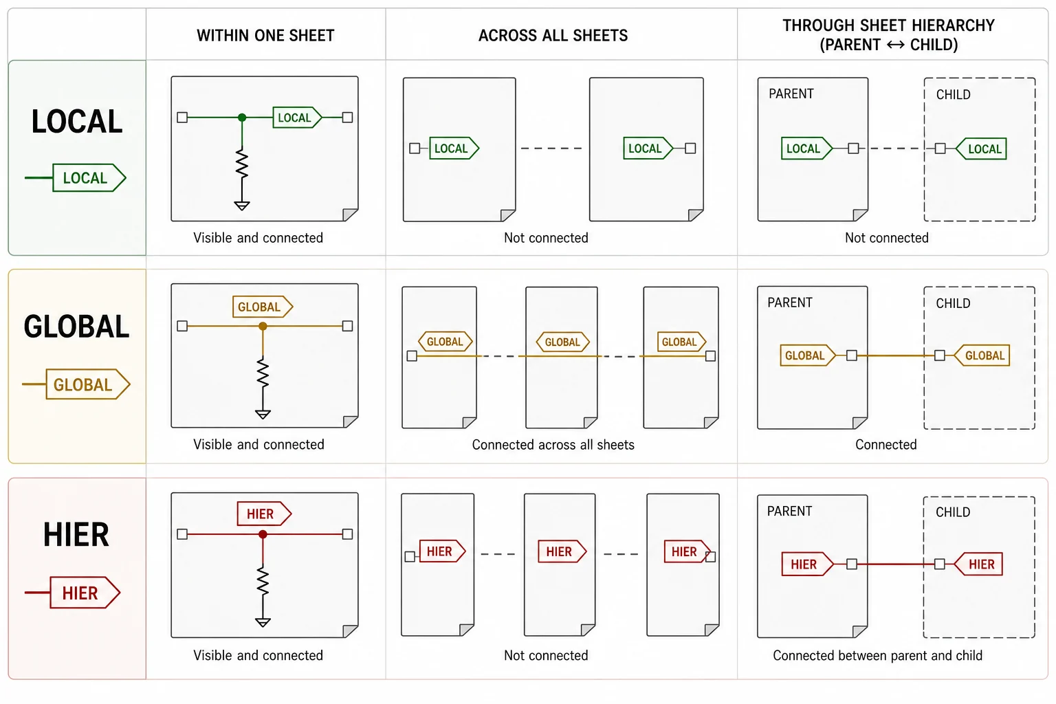
When Each KiCad Label Type Makes Sense
Use local labels for ordinary in-sheet routing
Local labels are the cleanest option for most signals. If an op-amp feedback node, MOSFET gate drive, or sensor bias trace never needs to leave the page, keeping it local reduces the chance that another sheet will accidentally claim the same name later. Local labels also make review easier because they do not imply hidden project-wide connectivity.
Use global labels only for signals that are meant to be global
Power rails and a few control nets often deserve global labels, but many projects use them too freely. If every control signal becomes global, sheet hierarchy stops telling the truth about the design. That becomes painful during debug, because a net name on page seven may actually be driven by a block on page two with no obvious boundary in between.
A practical rule is this: if a reviewer would ask, “Why does this signal need to exist everywhere?” it probably should not be global.
Use hierarchical labels to define interfaces between blocks
Hierarchical labels are what keep larger KiCad projects disciplined. They force signals to cross sheet boundaries through explicit ports instead of invisible same-name shortcuts. For power-conversion blocks, MCU subsystems, analog front ends, or connector breakout sheets, that explicit interface is usually worth the extra setup because it makes design ownership and debug boundaries much clearer.
Common Labeling Mistakes That Create Real PCB Problems
Reusing short generic names. A label like EN or OUT is easy to type and hard to audit. On a larger design, it invites accidental collisions.
Making local control signals global. This often happens when someone wants to avoid drawing sheet ports. The schematic gets faster to edit and slower to trust.
Renaming a net without checking downstream expectations. Connector tables, test notes, firmware pin maps, and layout constraints may still reference the old name.
Using labels to hide unresolved architecture. If the sheet only works once every wire disappears behind global names, the project likely needs cleaner block boundaries, not just cleaner graphics.
These mistakes are not only schematic problems. Net names often feed the PCB editor, fabrication notes, probe naming, or test documentation. A sloppy label can survive all the way into bring-up, where it turns into the wrong testpoint name, the wrong connector pin assumption, or a review miss on a mixed-signal board.
A Labeling Workflow That Stays Readable During Review
If you want labels that survive team review and board debug, a small amount of naming discipline goes a long way:
Prefer descriptive names tied to function, not position. FAN_TACH is better than SIG3.
Reserve global labels for rails and a short list of intentionally shared nets.
Name hierarchical ports from the perspective of the block interface, not only the local pin name.
Keep analog, power, and fast digital nets visually separated even when labels remove long wires.
Run ERC after interface changes, not only at the end of the project.
This is the same discipline that makes later layout and troubleshooting easier. ReversePCB readers who already care about schematic design quality, EDA workflow choices, or reading schematics without guesswork usually discover that label scope is one of the quiet details that separates a tidy-looking project from a maintainable one.
Use Labels to Clarify Intent, Not to Hide It
The best answer to how to make labels in KiCad is not “place text on the wire.” It is “pick the scope that matches the design boundary, then name the net so another engineer can review it quickly.” Once you think that way, labels stop being a shortcut and start becoming part of the design documentation.
FAQ
Should I use global labels for every repeated signal in KiCad?
No. Global labels are best reserved for rails and intentionally shared nets. If a signal only belongs inside one block or should cross sheets through a defined interface, local or hierarchical labels are usually safer.
What is the difference between a local label and a hierarchical label in KiCad?
A local label names a net inside the current sheet. A hierarchical label is meant to pass that signal through a sheet boundary so the connection stays explicit at the parent-child interface.
Why does ERC matter after changing labels in KiCad?
Because changing a label can change connectivity without changing the visible drawing very much. ERC helps catch unintended net merges, missing drivers, or naming conflicts before the schematic reaches layout.
How should I name nets in KiCad so they stay readable later?
Use short names tied to function, such as ADC_IN, USB_CC1, or MOTOR_FAULT. Avoid vague labels like IN, OUT, or TEST unless the context is extremely limited and local.