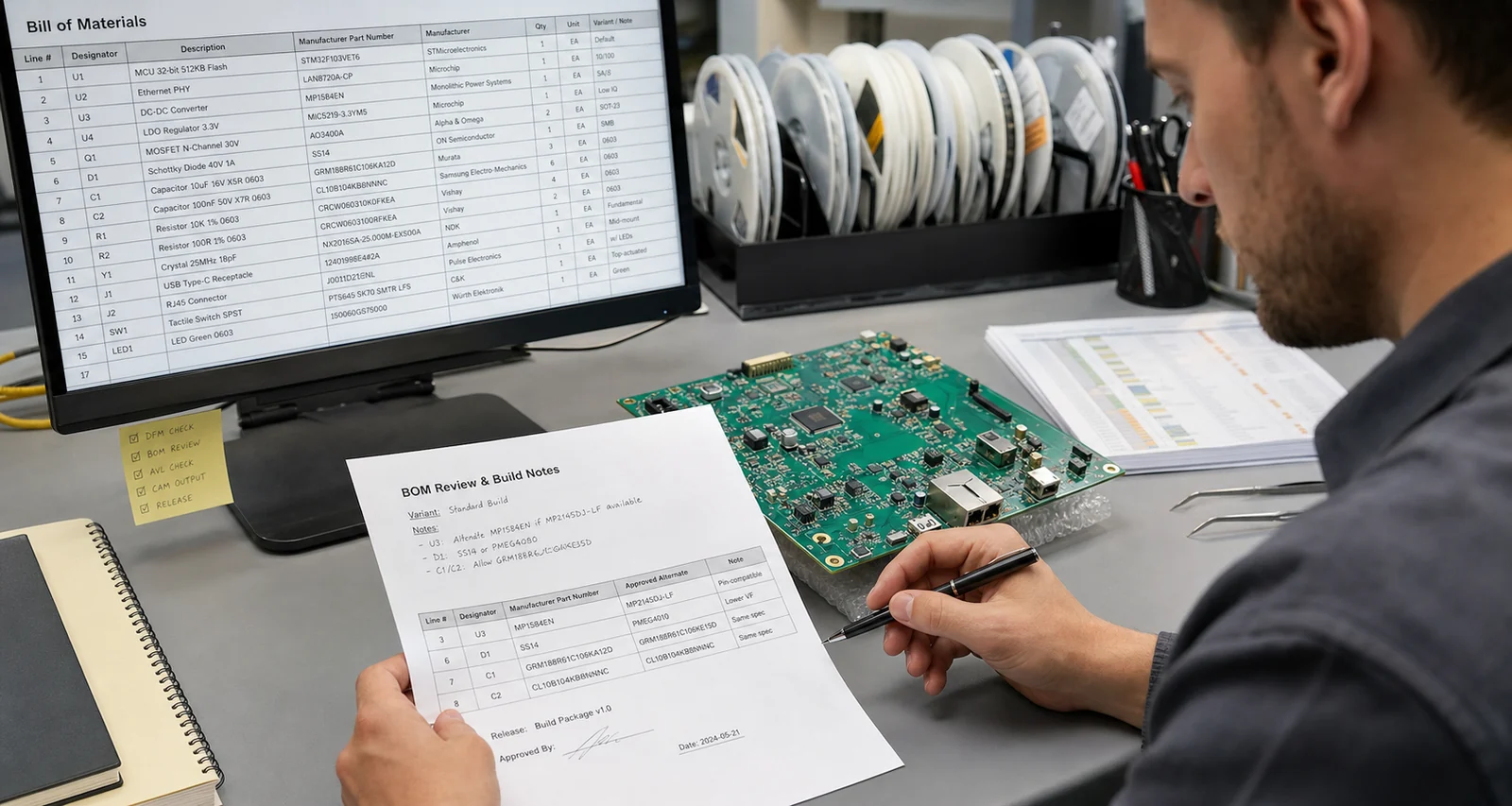
There are many articles on how to convert Gerber to PCB on the Internet, but most of them simply list a few steps. This article aims to introduce the process of Gerber conversion PCB in more detail, so that engineers can have a clear understanding of this “reverse engineering” process.
How to Generate PCB from Gerber?
Altium Designer comes with a tool similar to CAM350 called Camtastic. It can complete reverse engineering from Gerber to PCB. Below is a video guide:
Step 1: Create a new Cam document
To do this, please click File » New » CAM Document:

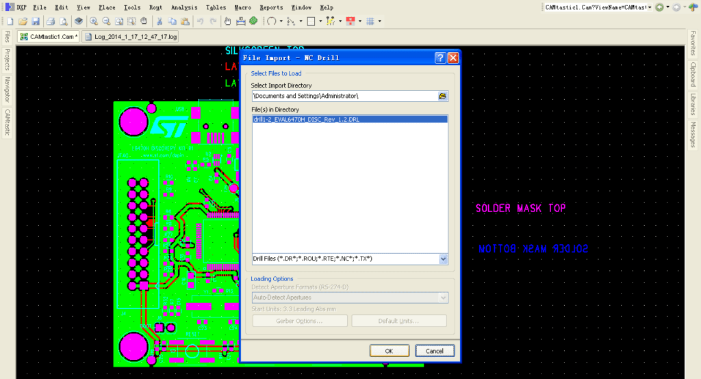
Step 2: Import Gerber and NC Drill

This is a critical step. If you only import Gerber but not NC Drill, the netlist cannot be decompressed later. If there is an IPC Netlist, it can also be imported together, so that when the netlist is decompressed, the name of the netlist will be the same as the source design, and the system will customize the name of the netlist by default.
In Preference, you can define the file extensions recognized by CAM. If you want to import Allegro or Expedition’s Gerber, you can add the corresponding extension here for quick identification.

After the import is complete, you can view or edit the Gerber file in AD:

Step 3: Layer Mapping
This is also a critical step. Click Tables » Layers to open the mapping interface:

The Gerber layer on the left must map correctly to the PCB layer in the Type column. The mapping of the signal layer is particularly important: the top layer/bottom layer are mapped to Top/Bottom respectively; the middle signal layer is mapped to Internal; the internal electrical layer is mapped to Pos Plane/Neg Plane.
Besides that, the TXT file of NC Drill also needs to be correctly mapped to Drill Top/Bottom/Int.
Step 4: Layer Order
Once the layers are mapped, the Create / Update Layer Order dialog will pop up (also accessible via the Layer » Order menu):

Here, it is necessary to define the physical order of all signal layers (including Top, Bottom, intermediate signal layer and internal electrical layer). This step is also quite critical. If there are blind and buried holes, if the definition is wrong here, it will directly lead to errors in PCB export. Remember, the Physical Order of the Top layer is always 1, and the order of other layers follows the actual layer structure and so on. Numbers in Physical Order cannot be repeated.
Step 5: Extract Netlist
If there is no problem with the above steps, the netlist information in the PCB can be deduced through Gerber and NC Drill. Click the Tools » Netlist » Extract menu to get the netlist of the PCB:

Step 6: Export PCB
The last step is to export the PCB. If the Net List or other information is missing, the Export to PCB menu is gray and cannot be clicked.

Engineering checks for Gerber to PCB reconstruction and verification
Before using Gerber to PCB reconstruction and verification in a PCB, firmware, repair, or validation workflow, confirm the details that usually decide whether the design works reliably instead of only reading the headline specification.
Design and troubleshooting checklist
| Area | What to check | Why it matters |
|---|---|---|
| File set | Check copper, solder mask, silkscreen, drill, aperture, outline, and IPC netlist files | Missing fabrication layers make the reconstructed PCB unreliable |
| Net recovery | Compare Gerber-derived nets with schematic intent, component pads, and drill connectivity | Gerbers are manufacturing data, not a complete design database |
| Output review | Verify scale, units, layer polarity, board outline, and plated/non-plated holes | Conversion errors often appear as mirrored layers or wrong drill interpretation |
These checks help connect the search intent around Gerber to PCB converter with practical board-level decisions, component selection, and failure analysis.