Blog Center
Learning from our posts in different topics: development case of chips, reverse engineering applications, ic programming tutorials, and more. Our team of experienced PCB experts are here to answer your queries and help you in any way possible.
Reading by Post Topics:
Post Showcase:

Reverse Engineering vs Forward Engineering
In the world of manufacturing and software, it’s not uncommon to hear words like reverse engineering or forward engineering. But what do those terms mean, and how do they apply

RF Circuits Explained: Basics & Working Principles
New to RF? Understand radio frequency circuits: components, impedance matching, and signal propagation. Applications in wireless devices. Beginner’s guide inside!

What is a High Frequency PCB?
When it comes to electronics, “smaller is better” is a common phrase that engineers often find themselves repeating. Engineers have been able to implement smaller components, through the use of

Through Hole vs Surface Mount
How many do you know about through hole vs surface mount? They are two ways to connect electronics components in pcb assembly (PCBA). They are cost-effective and reliable methods of

How to Create Schematic Symbol?
What is the schematic Symbol? A schematic symbol is a graphical representation of an electrical or electronic component. There are many schematic symbols in schematic library. And the schematic library

How to Create a PCB Library: Step-by-Step
Build PCB libraries: component footprints, symbols, and 3D models. Tools for Altium/KiCad and version control. Essential for efficient design. Tutorial inside!

How to Create a PCB BOM: Step-by-Step Guide
Master PCB BOM creation: component listing, part numbers, and sourcing. Tips for accuracy, cost optimization, and manufacturability. Download template inside!
IC Packaging and IC Testing Market Landscape Analysis
IC testing is to detect whether the chip has design defects or physical defects caused by the manufacturing process. The process can be conducted by using various test methods. IC

How to Reduce Power Supply Noise in Circuit Board?
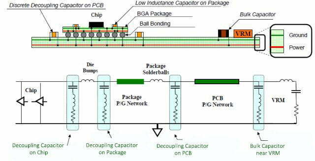
Power Supply Noise is a kind of electromagnetic interference (EMI) from the power distributor system. the frequency spectrum of its conducted noise is about 10kHz~30MHz, up to 150MHz. This noise

Effective PCB Footprint Strategies
What is PCB Footprint? PCB footprint, is the arrangement of pads used to mount a specific component to a printed circuit board. The footprint defines the outline of the component

IC Programming Guide: Tools & Processes
Programming integrated circuits: methods (JTAG, SPI), tools, and firmware flashing. Learn to debug and update ICs in embedded systems. Step-by-step inside!

PCB Layout Guidelines For A Successful Design
Master PCB layout: trace width, ground planes, and component placement. Tips for signal integrity, thermal management, and manufacturability.
