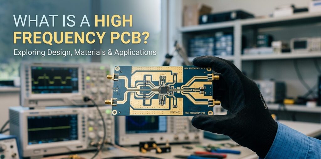
When it comes to electronics, “smaller is better” is a common phrase that engineers often find themselves repeating. Engineers have been able to implement smaller components, through the use of high-frequency PCB, which allow for smaller devices.
What is High Frequency PCB?
A high frequency PCB is a printed circuit board that is designed to operate at high frequencies. These boards are typically made with special materials and have special design features to minimize signal losses and ensure reliable operation at high speeds.
Frequency Formula
For high-frequency circuit pcb, the following formula is used to define the emission bandwidth of the signal, sometimes also called the EMI emission bandwidth:
F=1/(Tr*π)
“F” is the frequency (GHz); “Tr” (nanosecond) refers to the rise time or fall of the signal time.
Usually when F≥1GHz, it can be called a high-frequency circuit. According to this formula, it can be calculated that when the rise time of the signal is less than about 0.318ns.
high frequency PCB characteristic
- HF PCBs have small DK and better signal integrity than lower frequency PCBs.
- More resistant to crosstalk and electromagnetic interference.
- They can handle higher data rates.
- More expensive than lower frequency PCBs.
- Excellent impact resistance, chemical corrosion resistance, and heat resistance.
high frequency PCB design guidelines
1. Multi-layer boards routing
High-frequency circuits often have the characteristics of high integration and high density. Using multi-layer routing in pcb high frequency board is an effective way to reduce signal interference. During PCB Layout, use the intermediate layer to set the shield. This can effectively reduce parasitic inductance and shorten the transmission length of the signal. At the same time, it can also greatly reduce signal cross-interference and the like. All of these are beneficial to the reliability of high frequency circuits.
2. Avoid annular traces
All kinds of high-frequency signal traces should not be annular. If it cannot be avoided, the annular area should be kept as small as possible.
3. Reduce curved leads
It’s better to use straight leads in high-frequency circuit routing. You can also use a 45-degree polyline or a circular arc if needed. As a result, it can reduce the external emission and mutual coupling of high-frequency signals.
4. Reduce vias between layers
According to the measurement, a via can bring about 0.5pF of distributed capacitance. So, it’s able to improve speed and reduce the possibility of data errors, by reducing the number of vias can significantly.
5. Use short traces
In high frequency pcb traces, the longer the trace length, the higher the radiation intensity. This makes it easier to couple to nearby components. Therefore, short traces are better for high-frequency signal lines such as clocks, crystal oscillators, LVDS lines, USB lines, and HDMI lines.
6. Isolate the ground wire of digital and analog signals
The electric potential of the ground wire in the high-frequency digital signal is different from that in the analog signal, and there is a certain voltage difference between them. Moreover, the ground wire in high-frequency digital signals often has rich harmonic components. When the ground wires of the digital signal and the analog signal are directly connected, the harmonics of the digital signal will interfere with the analog signal through the ground wire coupling. Therefore, the ground wires of analog and digital signal must be connected to the common ground wire by using high-frequency choke beads. Or you can connect them with single-point in a suitable location.

7. Add HF decoupling capacitors
Place a decoupling capacitor near the power pin of each IC block to effectively suppress the interference of high-frequency harmonics on the power pins.
high frequency PCB application
Some potential applications for high frequency PCBs include:
- – military and aerospace applications
- – telecommunications
- – high speed digital devices
- – medical devices
- – Mobile phones
- – Satellite communications
- – Wi-Fi and other wireless networks
- – High speed computer networks
- – Radar and other electronic warfare systems
- – Medical imaging systems
High Frequency vs RF
There are two main types of electromagnetic waves: high frequency (HF) and radio frequency (RF). HF waves have a higher frequency than RF waves and can therefore carry more information. However, HF waves are also more susceptible to interference and can be absorbed by objects more easily than RF waves.
Benefits of High Frequency PCBs
As mentioned above, smaller is better when it comes to electronics. However, smaller boards can be harder to implement, especially if they are using low frequency signals. With high frequency PCBs, engineers are able to implement smaller boards and smaller components, making it easier to create smaller devices. RF boards can be used to transfer data at high rates, making it ideal for applications such as WiFi routers, cellular phones, and computer networks. It’s also useful in medical devices that send data, such as medical imaging devices, electrocardiograms (ECG), and other medical equipment.
Drawbacks of High Frequency Printed Circuits
The only real drawback to high frequency PCBs is that they operate at much higher frequencies than low frequency PCBs. This means that engineers must be careful as to what signals they are using as higher frequencies are more susceptible to noise. Another thing to mention is that high frequency PCBs cannot be routed with conductive materials, such as copper, as this will cause a short circuit. For this reason, high frequency boards must be routed with non-conductive materials such as polyimide-based materials.
High Frequency PCB Materials
There are a few things to consider when choosing high frequency PCB materials. The dielectric constant (Dk) and Dissipation Factor (Df) of the material are important properties to consider. The Dk of a material determines how well it can store electrical energy, while the Df determines how much energy is lost as heat. Materials with a low Dk and Df are ideal for high frequency applications.
FR-4 is a common dielectric used in PCBs. It has a Dk of around 4.5 and a Df of around 0.02. While FR-4 is a good general purpose dielectric, there are other materials that may be better suited for specific applications. For example, Rogers RO4003C has a Dk of 3.48 and a Df of 0.0037. This makes it a good choice for RF applications where low loss is important.
The table below shows some commonly used materials for making high frequency PCBs:
Another important consideration when choosing high frequency PCB materials is the thickness of the dielectric. The thicker the dielectric, the higher the capacitance. This is important to consider because the capacitance of a PCB affects the impedance. In general, it is best to use the thinnest dielectric possible while still maintaining the required capacitance.
When choosing high frequency PCB materials, it is important to consider the Dk, Df, and thickness of the dielectric. Using a material with a low Dk and Df will help to reduce losses, while using a thin dielectric will help to keep the impedance low.
Conclusion
High frequency boards operate at higher frequencies than low frequency boards and are used in wireless communication devices and computer networks. High frequency PCBs help engineers create smaller devices and also allow for greater data transmission rates. However, high frequency PCBs must be routed with non-conductive materials and cannot be routed with conductive materials such as copper.