Power Supply Noise is a kind of electromagnetic interference (EMI) from the power distributor system. the frequency spectrum of its conducted noise is about 10kHz~30MHz, up to 150MHz. This noise can interfere with the normal operation of electronic devices and can cause signal distortion. So, how can you reduce noise in your power supply? To answer this question and help you further understand the principles of reducing noise in power supply, we have come up with this blog post. Let’s get started!
What Is power distributor system (PDS)
A power distributor system (PDS) is a device that distributes power to multiple devices or circuit board components. The poor PDS design will cause structural resonance, and the deterioration of power quality. Usually, the PDS system consists of both the circuit system and the electromagnetic field (EMF) system. And the EMF contains the power supply and the ground plane. The figure below is a schematic diagram of a PDS.

As image shows above, power supply noise is generally generated from the IC. Then, it goes through the connection between the substrate Via and the solder balls on the package. Finally, it reaches the power supply system of the PCB.
Types of Noise in Power Supply
1.Harmonic distortion
Harmonic distortion is a type of waveform distortion when a signal is amplified. Improper biasing, amplifier overloading, and impedance mismatching can all cause harmonic distortion. In addtion,it can also occurs when an analog signal is converted to a digital signal.
2. Voltage Spike
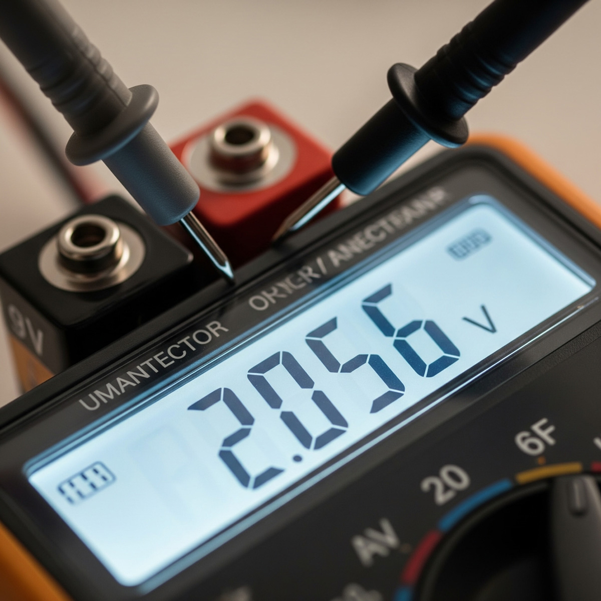
Voltage, current, and energy spikes are rapid, short-lived electrical transients in an electrical circuit. These electrical transients can create noise in the form of spikes in current. A voltage spike usually has a 6000V peak value and a duration from 1/10,000th of a second to 1/2 cycle (10 ms). The electrical transients are mainly due to lightning strikes, arcing, static discharge or switching operations of large electrical equipment. Voltage spikes often occur in steel mills, thyristor equipment, spark equipment, electric locomotives, etc. It will destroy the switching power supply, input filter, rectifier and even the main vibration tube of the industrial computer.

3. Ground Bounce Noise
Ground bounce noise (GBN) is a phenomenon that can occur in electronic circuits. When a signal line is connected to a ground plane with a high impedance. The high impedance can cause the signal to “bounce” off the ground plane, causing interference and noise.

We designed a PDS and made 3 comparison groups: a single Package, a single PCB, and the entire PDS system. The purpose is to measure the difference in GBN between them. In this process, we need to use the tools include network analyzer, Microtechprobe station, and GS probe.

From the measurement results in the above figure, we can see that the GBN values of the three PDS structures are quite different.
First of all, in the single Package mode, GBN behaves like a capacitor before 1.3Ghz, and the resonance mode is generated after 1.5Ghz;
Secondly, in the case of single PCB mode, GBN has resonance modes after 0.5Ghz, like 0.73Ghz (TM01), 0.92Ghz (TM10), 1.17Ghz (TM11), the GBN behavior is worse than that of single Pkg.
Finally, in the mixed structure of Package and PCB, the GBN frequency is three more resonance points than a single Package before 1.5Ghz. These noise resonances come from the PCB and are coupled to the Package’s power supply through solder balls, Via, etc. It will affect the ICs in the package more, but different from single package or PCB structure.
How to Reduce Noise in Power Supply?
There are a few ways to reduce noise in your power supply, including decoupling capacitors, filtering noise at the source. Here we will main discuss decoupling capacitors section.
Optimizing Decoupling Capacitors
An effective way to suppress power plane noise is to optimize decoupling capacitors. It contains capacitor size, capacitor location, capacitor ESR, capacitor ESL, and the number of capacitors.
1. Ideal location for decoupling capacitors
In order to analyze the influence of decoupling capacitor position on power supply noise, we add decoupling capacitors on Package and PCB respectively, and then measure GBN.

First of all, in the 0.5Ghz range, it can greatly reduce the structural impedance and reduce GBN interference no matter adding decoupling capacitors or not on the Package and PCB.
Second, in 0.5Ghz ~ 2Ghz range, we add decoupling capacitors both on the Pkg and PCB. They come with the same effect on noise suppression. However, you’ll find there’s an additional resonance point near 0.8Ghz, if you only add capacitors on the PCB. It is even worse than no adding capacitors. Therefore, we need to add decoupling capacitors both on the Pkg and PCB at the same time.
Third, from 2Ghz to 5Ghz, it’s nearly no helpful to reduce power supply noice by addding capacitors. Because this freqency range is larger than the resonance frequency of the capacitor itself.
2. Effect of Decoupling Capacitor ESR
On the mixed structure of the package and PCB, place 12 decoupling capacitors and change their equivalent series resistance (ESR). The simulation results are shown in the figure below. You will find that the noise curve becomes flatter, as the ESR value increases. This result tell us that increasing ESR is beneficial to suppress power supply noise.

3. Decoupling capacitor ESL
On the mixed structure of the Package and PCB, place 12 decoupling capacitors and change their Equivalent series Inductance (ESL). The simulation results are shown in the figure below. You’ll find that the resonance point amplitude become larger, as ESL value increases. As a result, only smaller ESL of decoupling capacitors is helpful for reducing noise.

4. Number of decoupling capacitors
In a single package structure, we do 6 time test and place different numbers of capacitors every time on the package.


Measurement result:
Between 0 and 200 MHz, 4 and 8 decoupling capacitors reduce the power supply’s noise. A new resonance point occurs near 400 MHz and the subsequent resonance point occurs at a higher frequency.
In addition, the power supply’s noise is also reduced when placing 12 to 52 decoupling capacitors. The resonance point near 400 MHz is getting smaller and the high-frequency resonance point occurs at a higher frequency. As a result, the noise of the power supply will decrease, as the number of capacitors increases.
5. Effect of Decoupling Capacitor Capacitance
On the combined structure of Package and PCB, place capacitors with different capacitance values. The simulation results are as follows:

Compare adding 100nF and 100pF:
- Between 0 and 300Mhz, 100n large capacitor has better suppression effect;
- 500~800Mhz, 100p small capacitor has better effect;
- Adding a 100n capacitor will resonate with the entire system structure at 400Mz;
- When using 100n+100p, 200~600Mhz, it is worse than simply using 100n and 100p, and lower frequency or higher frequency is not better than a single capacitance value;
- When three capacitance values of 100n+1n+100p are used, more resonance points are generated.
Special care must be taken in electronic systems, if the noise generated by the circuit is just at the resonant frequency, the noise is amplified and affects or radiates to the signal. Therefore, the selection of the capacitance value should be determined according to the frequency band to be suppressed. After the frequency band is determined, the capacitor should be selected according to the resonance point of the capacitor. The lower the ESL and ESR of the capacitor, the better.
6. Effect of PCB thickness
First, the distance between the fixed PCB power supply and the ground plane is 0.7mm, and the thickness of the Package power supply layer is changed to 1.6mm, 0.8mm, 0.4mm, and 0.15mm, and the results are shown in the figure.
When the thickness of the Package power supply layer is getting higher and higher, the first zero point moves to the low frequency. From the previous conclusion, the noise before 2Ghz comes from the PCB, and from the results, the noise coupled from the PCB also becomes larger.
After 2Ghz, it is mainly affected by the package. It can be seen that the noise also increases with the thickness, so the thickness of the acknowledge power plane has a great influence on the S-parameters.

Next, we fixed the thickness of the Package to 0.15mm, and changed the thickness of the PCB to 0.15mm, 0.4mm, 0.8mm, and 1.6mm, respectively. The effect of the PCB thickness on the S parameter is shown in the below figure.

We can see that the thickness of the PCB power layer has little effect on the overall trend. Only the low-frequency part has little difference. The first zero point of the thickness increases with a small high-frequency movement, and the high-frequency part has only a slight difference.
7. The effect of capacitor placement distance
We know that the closer the decoupling capacitor is to the noise source, the better, because it reduces the inductance value from the capacitor to the noise source. And in this way, the capacitor absorbs the surge faster, reduces the noise, and achieves the function of stabilizing the voltage. Similarly, reducing the thickness of the power layer can reduce the parasitic inductance of the power plane, which can also play the same role.

In the simulation, we change the distance between the capacitor on the package and the test point, which are 1.7cm and 0.2cm respectively. The thickness of the package and the PCB power layer is divided into two cases. The first package is 0.15mm and the PCB is 0.7mm. In the second case, Package 1.6mm and PCB 0.7mm, capacitor 100nF, ESR 0.04ohm, ESL 0.63nH.

It is known from the simulation results that we can reduce the influence of noise by reducing the thickness of the Power layer of the Package, when the capacitor cannot be placed near the noise source due to package structure or wiring problems.
Conclusion
In this post, we introduce about how power supply noise happen and how to reduce its’ influence on PCB.