HDI PCB Guide: Design & Applications
HDI (High-Density Interconnect) PCBs: layers, microvias, and advanced manufacturing. Ideal for mobile devices and wearables. Expert insights inside!
If you’ve ever listened to an uncle playing blues guitar or a friend strumming a cheap plastic ukulele, you probably know what harmonic distortion is. It sounds like a very slight buzz, hiss, or whiz in the background of their performance. That is because these instruments aren’t able to produce their notes without some kind
Harmonic Distortion: What It Is and How To Prevent It? Read More »
In the world of manufacturing and software, it’s not uncommon to hear words like reverse engineering or forward engineering. But what do those terms mean, and how do they apply to you? Let’s take a look at what these terms mean and how they can be used in your business. These are two techniques that
New to RF? Understand radio frequency circuits: components, impedance matching, and signal propagation. Applications in wireless devices. Beginner’s guide inside!
RF Circuits Explained: Basics & Working Principles Read More »
When it comes to electronics, “smaller is better” is a common phrase that engineers often find themselves repeating. Engineers have been able to implement smaller components, through the use of high-frequency PCB, which allow for smaller devices. What is High Frequency PCB? A high frequency PCB is a printed circuit board that is designed to
How many do you know about through hole vs surface mount? They are two ways to connect electronics components in pcb assembly (PCBA). They are cost-effective and reliable methods of connecting electrical components with conductive pads, wires or copper bumps. In this blog post, let’s explore the pros and cons of these different techniques to
What is the schematic Symbol? A schematic symbol is a graphical representation of an electrical or electronic component. There are many schematic symbols in schematic library. And the schematic library is one of the important steps in pcb reverse engineering. Structure of Schematic Symbols There are several essential elements that constitute a schematic symbol: Profile
Build PCB libraries: component footprints, symbols, and 3D models. Tools for Altium/KiCad and version control. Essential for efficient design. Tutorial inside!
Master PCB BOM creation: component listing, part numbers, and sourcing. Tips for accuracy, cost optimization, and manufacturability. Download template inside!
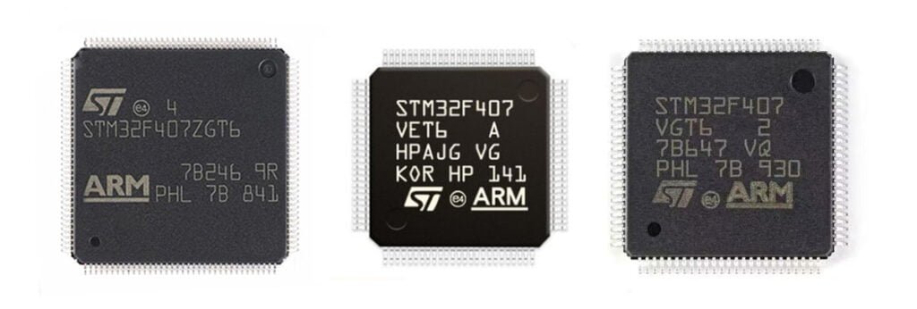
IC testing is to detect whether the chip has design defects or physical defects caused by the manufacturing process. The process can be conducted by using various test methods. IC packaging is the process of enclosing an integrated circuit (IC) in a protective package. This process protects the IC from damage and ensures that it
IC Packaging and IC Testing Market Landscape Analysis Read More »