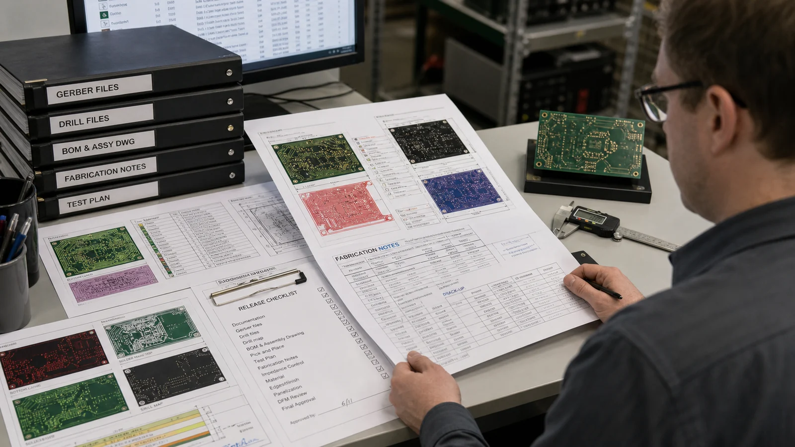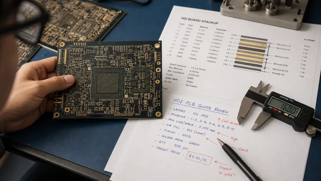
HDI PCB cost rarely jumps because of one dramatic line item. It usually climbs because several small design decisions all point the supplier toward extra lamination cycles, tighter imaging, more via processing, and slower inspection. A board that looks efficient in layout can become an expensive NPI build if the stackup, microvia structure, and assembly assumptions are still vague when the RFQ goes out. This guide explains what actually raises HDI PCB cost, where teams misread the quote, and how to reduce cost without quietly weakening yield or reliability.
HDI PCB cost is driven by process complexity, not just layer count
The most important cost shift in HDI work is that the board stops behaving like a conventional multilayer quote with finer traces. Once the design needs laser microvias, sequential lamination, stacked via structures, or aggressive escape routing under fine-pitch BGA fields, the supplier is no longer pricing ordinary copper and drilling alone. They are pricing process risk, registration control, coupon strategy, and the probability that the build will need more engineering attention before it reaches stable yield.
That is why two boards with similar outline size and similar component count can quote very differently. The expensive board is often the one that compresses too much density into one region, mixes demanding impedance targets with HDI build-up layers, or leaves the via strategy underspecified. If you only compare total layers, you miss the real cost drivers.
What usually raises HDI cost the fastest
Cost rises quickly when the design forces the fabricator into additional process steps that are difficult to run consistently. In HDI work, the quote often moves more on manufacturability details than on raw board area.
Laser microvia count and structure
Blind microvias are one of the main reasons an HDI build costs more than a standard multilayer board. A simple staggered microvia structure is usually easier to process than stacked microvias that require extra fill quality and tighter registration through repeated build-up cycles. If the breakout can be solved with fewer stacked transitions, the quote often becomes easier to stabilize. The cost question is not whether microvias are present. It is how many there are, how they are arranged, and whether they force extra process sensitivity under dense packages.
Sequential lamination count
Each lamination cycle adds time, tooling dependency, and yield exposure. Designers sometimes focus on routing success and forget that every build-up stage also asks the supplier to preserve alignment, hole quality, dielectric control, and copper integrity through another press sequence. That is why a stackup that looks elegant on paper can still become the expensive option if it needs more lamination stages than the signal problem really requires.
Fine line and imaging limits
Very small trace and space rules do not only affect etching. They also tighten what the shop must control during imaging, plating, and inspection. If the design uses HDI partly to support fine-pitch BGA escape but then pushes many ordinary nets into unnecessarily tight geometry, the board becomes harder to build without gaining much system value. Cost climbs again when narrow lines also carry controlled-impedance requirements, because material choice and dielectric thickness tolerance begin to matter more.
Via filling, capping, and planar surfaces
When HDI routing turns into via-in-pad or dense pad-adjacent microvia work, the price is affected by fill quality, cap quality, and final planarity rather than routing density alone. A supplier may be able to fabricate the board electrically, but if the microvia structure under a BGA or bottom-terminated package creates solder starvation, voiding, or uneven collapse, assembly cost returns through rework and first article delays. That makes the bare-board quote look incomplete if assembly realities were never part of the review.
Why BGA escape strategy can change the whole quote
Many HDI cost problems start under one or two packages. Once a fine-pitch BGA forces blind-via fanout, narrower neck-downs, and extra build-up layers, the rest of the board inherits that process complexity even if the remaining routing is ordinary. In practice, the cheapest HDI board is often the one that contains the demanding escape region instead of letting it reshape the entire stackup.
That is why package planning matters before procurement asks for final quotes. If the part can be replaced with a pitch that supports a cleaner fanout, or if the breakout can be reorganized to reduce stacked microvia usage, the savings can be more meaningful than negotiating a few percentage points from the board shop. ReversePCB already covers the routing rules of BGA package design; in an HDI cost review, those routing choices become purchasing decisions as well.
Assembly, inspection, and test can make a low board quote expensive
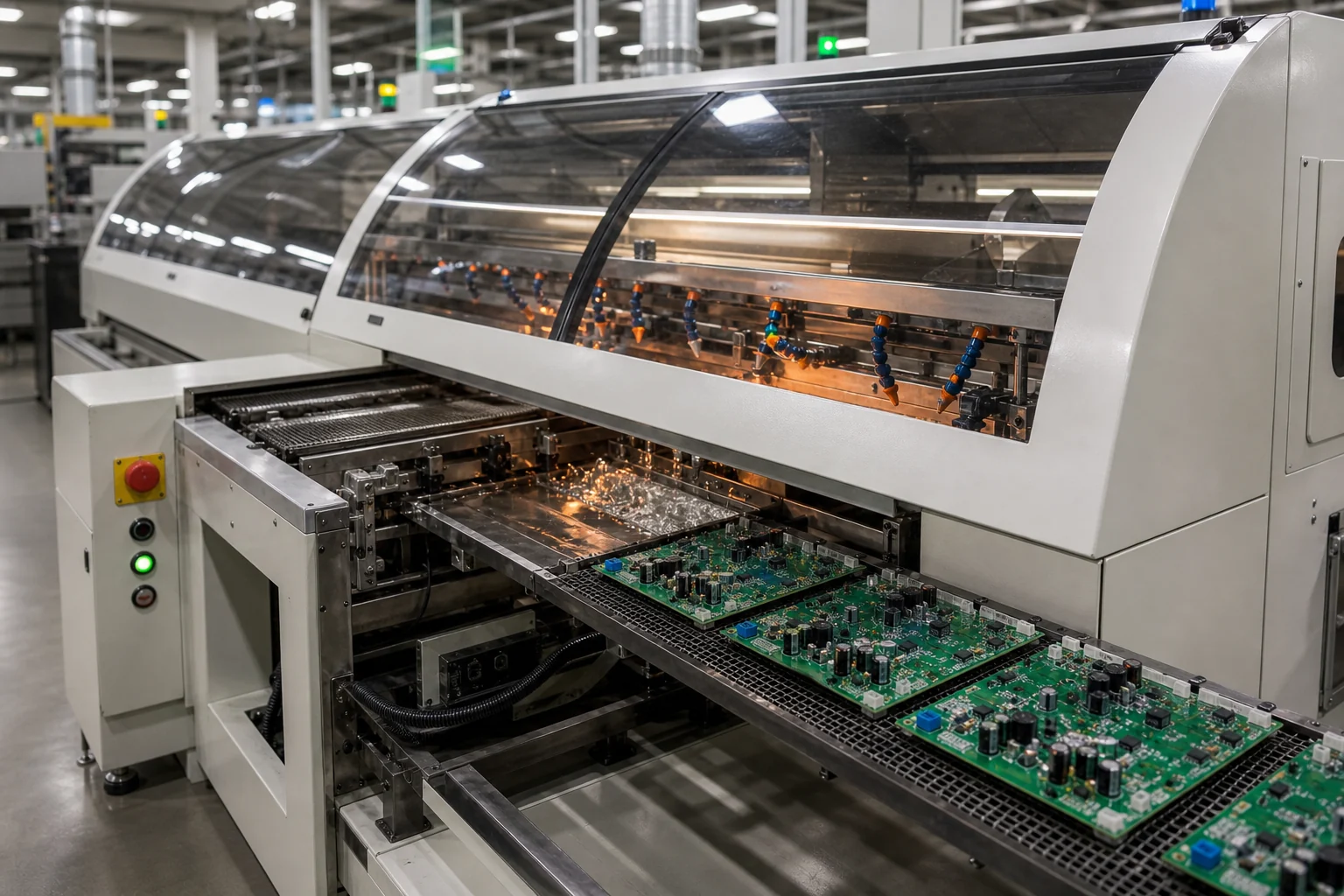
An HDI quote that looks attractive on bare-board cost alone may still be expensive at the PCBA stage. Dense component fields reduce probe access, complicate fixture design, and can push inspection toward X-ray-heavy checkpoints rather than routine optical confirmation. If the board uses filled microvias in pad fields, large thermal pads, or bottom-terminated packages with limited visual feedback, first article inspection time usually rises. That affects schedule and NPI cost even if the fabricator’s unit price looks competitive.
Repair realities matter too. Some HDI boards are not realistically reworked without high skill, local heating control, and a credible plan for pad integrity after component removal. A sourcing team that compares suppliers only on board fabrication price can miss the downstream cost of reballing, replacing parts near delicate microvia fields, or scrapping borderline assemblies that are not worth field repair.
How to reduce HDI PCB cost without creating a yield problem
The useful goal is not to make HDI cheap at any cost. It is to remove unnecessary complexity while protecting the density and performance that justified HDI in the first place. That usually means simplifying structure before negotiating price.
- Reduce stacked microvia usage where a staggered structure or a different escape path will still meet routing goals.
- Check whether every fine-line region really needs the tightest geometry, or whether only the BGA escape area does.
- Review whether one more signal layer on a simpler structure is actually cheaper than a more aggressive HDI build-up sequence.
- Keep controlled-impedance routing and HDI density reviews tied together so the stackup does not solve one problem by creating another.
- Ask assembly what package fields will need X-ray, special stencil tuning, or difficult rework before the board is released.
- Document the microvia, fill, cap, and planarity assumptions inside the RFQ instead of leaving them to interpretation.
Teams often save more by narrowing the difficult region than by trying to make the entire board heroic. If a local HDI area solves the package problem while the rest of the stackup stays conventional, yield and quote stability usually improve. For baseline context, compare the cost review against the published HDI PCB guide, the PCB via overview, and the newer standard PCB stackup tradeoff guide. Those references help separate true HDI requirements from habits carried over from previous layouts.
What a buyer should include in an HDI RFQ
An HDI RFQ needs more than a generic stackup request and Gerber set. If the supplier has to guess the via structure, acceptable registration margin, planarity expectation, or inspection hold points, the first quote may not be comparable across vendors. It is better to expose the hard parts early than to discover after award that one quote assumed staggered microvias while another silently priced stacked fill and cap work.
A practical RFQ package should state the intended microvia architecture, whether any via-in-pad features require fill and cap, which nets need impedance control, where dense BGA escape zones sit, and whether first article evidence such as coupons, X-ray samples, or process notes will be required. If lead time matters, ask directly whether the stackup depends on special material availability or whether the build can stay inside the supplier’s routine HDI process window.
Use HDI where it earns board area, routing freedom, or electrical margin
HDI PCB cost is easiest to justify when the design gains something measurable: a package escape that would otherwise fail, a smaller product envelope, cleaner routing for fast interfaces, or a better balance between density and signal control. It becomes harder to justify when HDI is used broadly without defining which constraint it actually solves. A disciplined HDI quote review asks a simple question at every expensive feature: does this step protect performance or manufacturability, or is it only compensating for an earlier layout shortcut?
FAQ
Why is HDI PCB cost higher than a standard multilayer PCB?
HDI cost rises because the board often needs laser microvias, sequential lamination, tighter imaging, more difficult registration control, and more inspection effort than a conventional multilayer build. The extra cost is usually tied to process complexity and yield management rather than copper area alone.
Do stacked microvias always make an HDI board more expensive?
Usually yes, because stacked structures are more demanding to fill, align, and verify than simpler staggered approaches. They can still be worth the cost when package density or routing constraints leave no cleaner option, but they should be used intentionally rather than by default.
Can an HDI PCB quote look cheap but still create high assembly cost?
Yes. Dense BGA fields, limited probe access, filled via structures, and heavier X-ray dependence can add first article, inspection, and rework cost even when the bare-board price looks reasonable. That is why fabrication and assembly assumptions should be reviewed together.
How can designers lower HDI PCB cost before sending an RFQ?
The best savings usually come from simplifying the via strategy, containing the densest escape region, avoiding unnecessarily tight geometry outside critical areas, and documenting microvia, impedance, and planarity requirements clearly. Price negotiation helps, but structure simplification usually has a bigger effect on stable yield and real program cost.