Gold Fingers PCBs are one of the most popular printed circuit boards (PCBs) used in electronics and computing applications. They are essential components of many electronic devices, from computers to smartphones. But what exactly are Gold Fingers PCBs and how do they work? In this blog, I will give you an overview of Gold Fingers PCBs, the benefits of using them, the types available, the applications, production standards, plating process, how to design them, testing, and troubleshooting.
Introduction to Gold Fingers PCBs
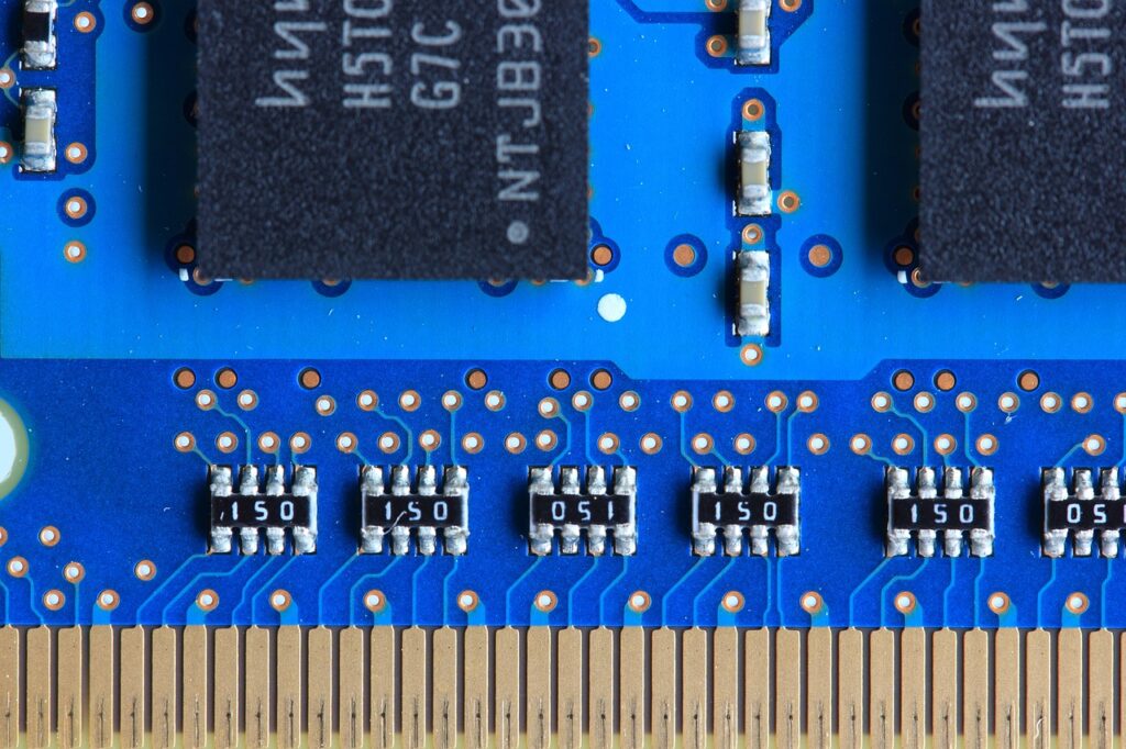
Gold fingers are a type of electrical connector that is used to connect a printed circuit board (PCB) to other components or another PCB. They are so named because the finger-like projections at the end of the connector look like gold. The gold-plated contact fingers are used to connect the board to other components such as memory, processor, and other integrated circuits. Gold Fingers PCBs are used in a variety of applications, such as computers, laptops, cell phones, gaming consoles, and other electronic devices.
Gold Fingers PCBs are popular because they provide excellent electrical conductivity, high durability, and corrosion resistance. Gold Fingers PCBs are also known for their ability to maintain their electrical properties over time and withstand the harsh conditions of the environment.
Overview of Gold Fingers PCBs
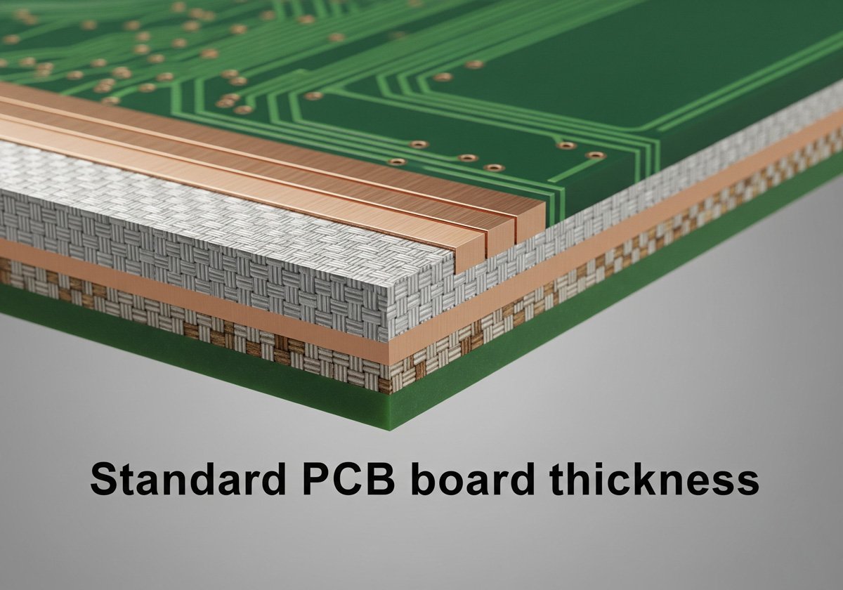
Gold Fingers PCBs are typically made of a thin layer of copper that is laminated onto a substrate. This substrate is then coated with a thin layer of gold. The gold-plated fingers are then connected to the PCB via electrical contacts.

The gold-plated fingers provide excellent electrical conductivity, allowing for the transmission of signals from one component to another. They are also highly durable, and able to withstand harsh conditions such as extreme temperatures and moisture. Gold Fingers PCBs are also resistant to corrosion, meaning that they can last for a long time without needing to be replaced.
What are the Benefits of Gold Fingers PCBs?
Gold Fingers PCBs offer several advantages to designers and engineers. They are highly reliable and provide excellent electrical conductivity. The gold-plated contacts are also highly durable, and able to withstand extreme temperatures, moisture, and other harsh conditions. Gold Fingers PCBs also provides excellent corrosion resistance, meaning that they can last for a long time without needing to be replaced.
Furthermore, Gold Fingers PCBs are also cost-effective. The gold-plated contacts are relatively inexpensive and can be reused multiple times. This makes them an ideal choice for designers and engineers who are looking to reduce costs.
Gold Fingers PCBs are also highly versatile. They can be used in a variety of applications, from computers and laptops to cell phones and gaming consoles. This makes them an ideal choice for designers and engineers who are looking to create products that are compatible with multiple platforms.
Types of Gold Fingers PCBs
Gold Fingers PCBs come in a variety of sizes and shapes. The most common type is the dual-layer Gold Fingers PCB, which is composed of two layers of copper and a layer of gold plating. This type of Gold Fingers PCB is often used in computers and laptops.
Another type of Gold Fingers PCB is the single-layer Gold Fingers PCB, which is composed of one layer of copper and a layer of gold plating. This type of Gold Fingers PCB is often used in cell phones and gaming consoles.
Finally, there is also the multi-layer Gold Fingers PCB, which is composed of multiple layers of copper and a layer of gold plating. This type of Gold Fingers PCB is often used in complex electronic devices.
What Are Gold Fingers Used for?
Gold fingers are primarily used in computer hardware and other electronics that require high-speed signal transmission. The gold coating helps reduce interference and crosstalk, which can lead to signal loss. It also reduces corrosion, which is important when dealing with electronics that may be exposed to moisture or other environmental conditions.
Gold fingers come in a variety of sizes, shapes, and configurations to accommodate different types of electronic components and connections. Some common types are edge connectors, pin headers, and D-sub connectors. Depending on the application, they can be soldered directly to the PCB or connected with a socket or plug.
In addition to being used in computers and other electronics, gold fingers are also used in gaming consoles, home entertainment systems, and other consumer electronics. They provide a secure connection between components while maintaining signal quality. Because of this, gold fingers are an essential component in any electronic device that needs high-speed signal transmission.
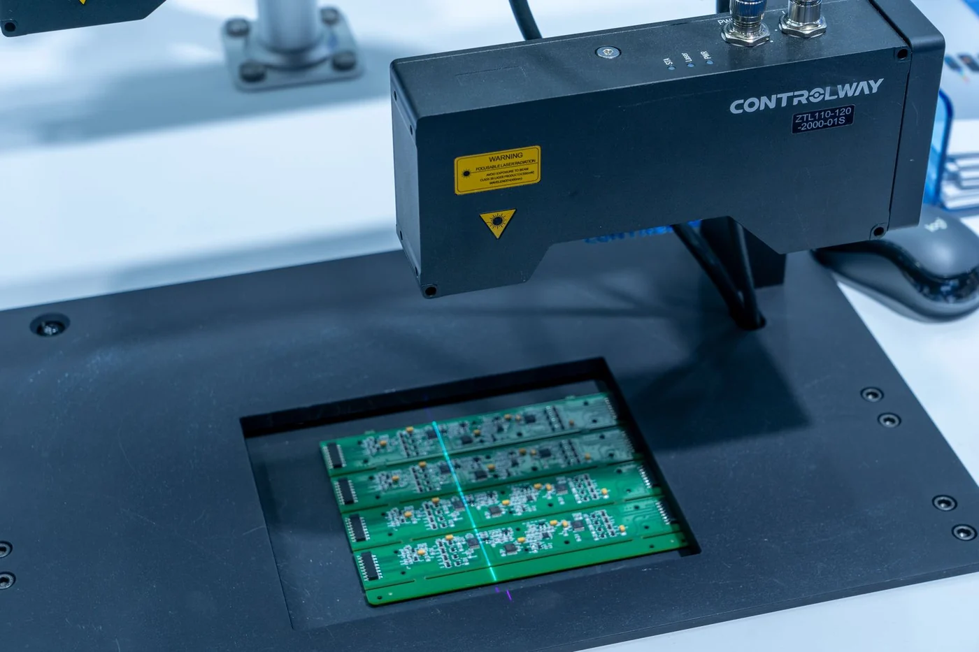
Gold Finger Production Standards
PCB gold fingers are used to create connections between boards and other devices. In order to ensure the reliability of these connections, it is essential to adhere to industry-standard production standards.
The International Printed Circuit Association (IPC) sets the standards for the production of PCB gold fingers and all other components in the electronic industry. These standards cover various aspects of the production process, from the design and manufacturing of the components to final testing. The IPC standards for PCB gold fingers require that all components must have smooth and even gold plating and a minimum thickness of 30 microinches on all exposed surfaces.
The IPC-A-600 standard is a visual acceptance standard used to evaluate the acceptability of bare printed circuit boards. It defines the criteria that must be met in order to ensure that a board meets the required electrical, mechanical, and cosmetic requirements. Specifically, the IPC-A-600 standard outlines the requirements for PCB gold fingers. According to the IPC-A-600 standard, PCB gold fingers must be free of any contamination, including corrosion, soldering flux, and other contaminants. Additionally, the gold plating must be uniform and fully cover the surface of the gold finger. The gold fingers must also be free of visual defects such as scratches, pits, or other irregularities. Finally, the gold thickness must meet the specified requirements for the type of connector used. Following these requirements will ensure that PCBs with gold fingers meet the required electrical, mechanical, and cosmetic requirements.
In addition to the IPC standards, manufacturers often also maintain their own internal quality control standards in order to ensure the highest possible level of product quality. This includes regular testing of the gold plating to verify its thickness and durability, as well as the use of high-quality materials and processes to ensure that all components meet the required standards. These measures help to guarantee that all PCB gold fingers produced meet the highest standards and provide reliable connections for years to come.
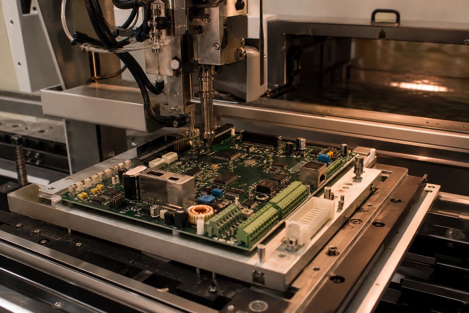
The Plating Process of PCB Gold Fingers
The plating process for gold fingers is a multi-step process that begins with a copper electroplating. A copper layer is applied to the board to provide a suitable base upon which the gold plating can be deposited. After the copper plating, an acid etch is used to remove any excess copper and create a rough surface texture. This rough texture will help the gold plating to adhere better.
Next, a thin layer of nickel is applied to the board to act as a bonding agent between the copper and the gold. After the nickel plating, the gold plating is applied and allowed to cure. The gold plating is typically applied in two layers, one that is thinner and one that is thicker. The thicker layer will be the visible layer of gold seen on the gold fingers.
Finally, the gold plating is sealed in place with a protective coating. This coating helps to protect the gold fingers from tarnishing and corrosion. It also prevents short-circuiting or arcing between the gold fingers and other components.
The plating process for gold fingers is a complex process that requires careful attention to detail to ensure the highest quality results. Properly plated gold fingers will provide reliable electrical connections and superior durability.
How to Design Gold Fingers PCBs
Designing Gold Fingers PCBs is not as difficult as it may seem. The first step is to determine the size and shape of the Gold Fingers PCB. The size and shape will determine the number of layers and the type of substrate used in the Gold Fingers PCB.
The second step is to determine the thickness of the gold plating. The thicker the gold plating, the better the electrical conductivity and durability of the Gold Fingers PCB.
The third step is to determine the size of the gold-plated contact fingers. The larger the contact fingers, the higher the electrical current that can be transmitted through them. However, the larger the contact fingers, the more expensive the Gold Fingers PCB.
The fourth step is to select the type of substrate used in the Gold Fingers PCB. The type of substrate used will determine the strength, flexibility, and durability of the Gold Fingers PCB.
Finally, the fifth step is to select the type of gold plating used in the Gold Fingers PCB. The type of gold plating used will determine the electrical conductivity of the Gold Fingers PCB.
Testing Gold Fingers PCBs
Once the Gold Fingers PCBs have been designed and manufactured, they must be tested to ensure that they are functioning properly. The most common method of testing Gold Fingers PCBs is the use of an ohmmeter. An ohmmeter is used to measure the electrical resistance of the Gold Fingers PCB.
The ohmmeter is connected to the Gold Fingers PCB and the electrical resistance is measured. If the electrical resistance is too high, it indicates that the Gold Fingers PCB is not functioning properly. Similarly, if the electrical resistance is too low, it indicates that the Gold Fingers PCB is not functioning properly.
Other methods of testing Gold Fingers PCBs include visual inspection, temperature testing, and electrical testing. Visual inspection is used to check for any defects in the Gold Fingers PCBs. Temperature testing is used to check the temperature resistance of the Gold Fingers PCBs. Electrical testing is used to check for any shorts or opens in the Gold Fingers PCBs.
Troubleshooting Gold Fingers PCBs
If the Gold Fingers PCBs are not functioning properly, there are a few steps that can be taken to troubleshoot the issue. The first step is to check for any shorts or opens in the Gold Fingers PCBs. This can be done by using an ohmmeter to measure the electrical resistance of the Gold Fingers PCBs.
The second step is to check for any defects in the Gold Fingers PCBs. This can be done by using visual inspection to check for any cracks, chips, or other defects in the Gold Fingers PCBs.
The third step is to check the temperature resistance of the Gold Fingers PCBs. This can be done by using temperature testing to check the temperature resistance of the Gold Fingers PCBs.
Finally, the fourth step is to check the electrical conductivity of the Gold Fingers PCBs. This can be done by using electrical testing to check the electrical conductivity of the Gold Fingers PCBs.
Conclusion
Gold Fingers PCBs are essential components of many electronic devices, from computers to smartphones. They offer excellent electrical conductivity, high durability, and corrosion resistance. Gold Fingers PCBs come in a variety of sizes and shapes and are used in a variety of applications.
When designing Gold Fingers PCBs, there are a few design considerations that must be taken into account. The Gold Fingers PCBs must be tested to ensure that they are functioning properly. If the Gold Fingers PCBs are not functioning properly, there are a few steps that can be taken to troubleshoot the issue.
I hope this blog has given you an overview of Gold Fingers PCBs, the benefits of using them, the types available, design considerations, how to design them, testing, and troubleshooting. If you have any questions about Gold Fingers PCBs, feel free to reach out to me and I’ll be happy to help.