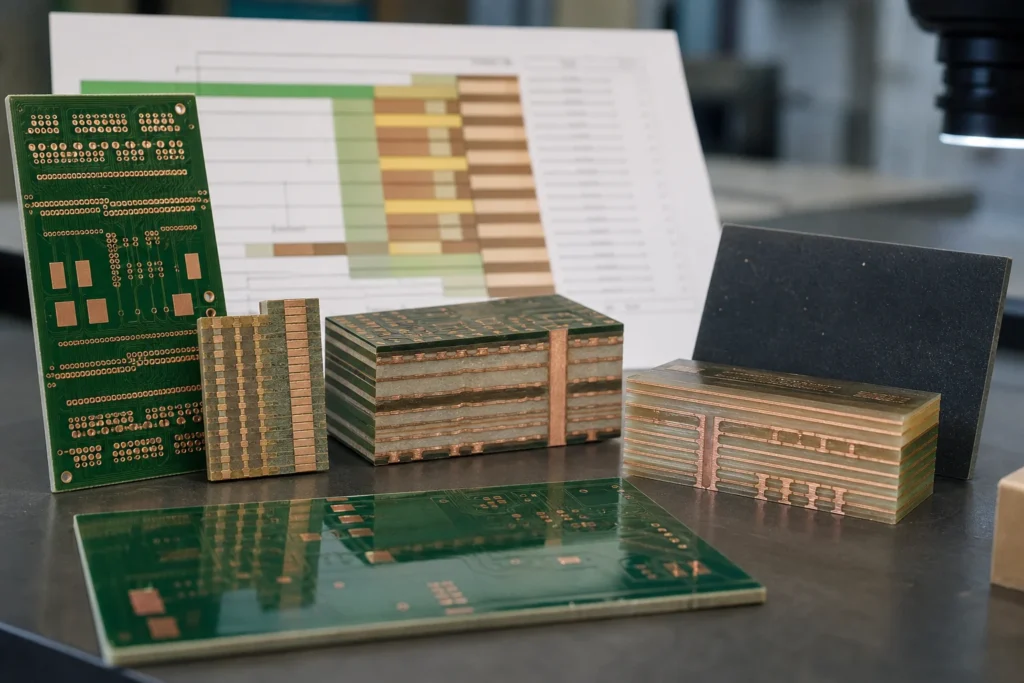
A standard PCB stackup is only standard until the design starts asking for cleaner return paths, tighter impedance windows, lower EMI, better thermal spreading, or a cheaper fabrication route. That is why a standard 2-layer PCB stackup, a standard 4-layer PCB stackup, and a standard 6-layer PCB stackup are not interchangeable defaults. Each one makes different promises about routing space, shielding, yield, and cost. This guide explains how common 2-, 4-, 6-, and 8-layer stackups are usually used, where they break down, and what to confirm before treating a vendor default as safe for production.
What people usually mean by a standard PCB stackup
In most quoting conversations, a standard stackup means a layer arrangement the board shop can build without special laminate sourcing, unusual foil combinations, or a long engineering review. That sounds convenient, but it does not mean the stackup is automatically right for your design. A vendor default may be tuned for throughput and material availability, while your board may care more about impedance control, return-path continuity, bow-and-twist margin, or reflow stability on a dense assembly.
That gap is where problems start. Teams often approve a “standard” stackup because it shortens the quote cycle, then discover late that the copper balance is poor for the component density, the prepreg thickness shifts the impedance target, or the plane allocation leaves too many signals crossing split references. A standard stackup is a starting point, not a waiver of engineering review.
When a standard 2-layer PCB stackup still makes sense
A 2-layer PCB stackup still works well for simple power products, low-speed controls, adapter boards, and cost-sensitive hardware where routing density is modest and EMI expectations are realistic. It is attractive because fabrication is straightforward, lead time is usually short, and inspection is easier than on a dense multilayer build.
The limitation is not just routing space. Once a board has mixed switching regulators, noisy interfaces, fine-pitch components, or several current loops fighting for the same return area, a 2-layer stackup stops being cheap in the full program sense. You may spend the savings back in jumpers, patch traces, EMC fixes, or mechanical rework. The right question is not whether 2 layers can be fabricated, but whether 2 layers let the circuit behave predictably after layout compromises begin.
Why the standard 4-layer PCB stackup is the practical baseline for many boards
A standard 4-layer PCB stackup is often the first layout that feels balanced instead of merely possible. It gives designers room for a dedicated reference plane, cleaner return paths, better power distribution, and fewer routing contortions around packages that would feel cramped on two layers. For many commercial and industrial products, 4 layers is where signal integrity, manufacturability, and cost stop fighting each other quite so aggressively.
That does not mean every 4-layer arrangement performs the same. If the signal layers sit too far from their reference planes, impedance drifts and emissions get harder to control. If copper usage is badly unbalanced, the stackup can invite warpage during lamination and assembly. The PCB stackup design basics still matter even when the layer count looks ordinary.
A standard 6-layer PCB stackup earns its keep when partitioning starts to matter
A standard 6-layer PCB stackup becomes useful when the board needs more than one clean signal environment at the same time. High-speed interfaces, tighter impedance goals, mixed noisy and sensitive sections, and denser BGA escapes often push a design into six layers long before the routing software runs out of tracks. The extra layers create room for better reference management, power segmentation, and shielding without resorting to fragile trace gymnastics.
This is also where “standard” can become misleading. One 6-layer proposal may prioritize routing convenience, while another places planes in a way that keeps stripline behavior and return paths more stable. If the board includes fast edge rates, RF sections, or ADC front ends sharing space with switching rails, the layer order matters as much as the layer count. A nominally standard 6-layer stackup that leaves critical traces referencing inconsistent planes can still behave like a rushed prototype.
What an 8-layer PCB stackup changes beyond adding more copper
An 8-layer PCB stackup is usually not chosen just because the routing got crowded. It is chosen because the design needs more control over field containment, reference continuity, rail distribution, or breakout density than 6 layers can deliver comfortably. At that point, the stackup decision affects EMI margin, crosstalk behavior, thermal spreading, and fabrication cost all at once.
The trap is treating 8 layers as automatic insurance. If the plane strategy is weak, extra layers can still produce poor return paths, unnecessary via transitions, and avoidable assembly cost. The value comes from disciplined layer assignment, not from copper count alone. That is especially true on boards heading toward radar, RF, or other high-frequency work where the signal environment is far less forgiving.
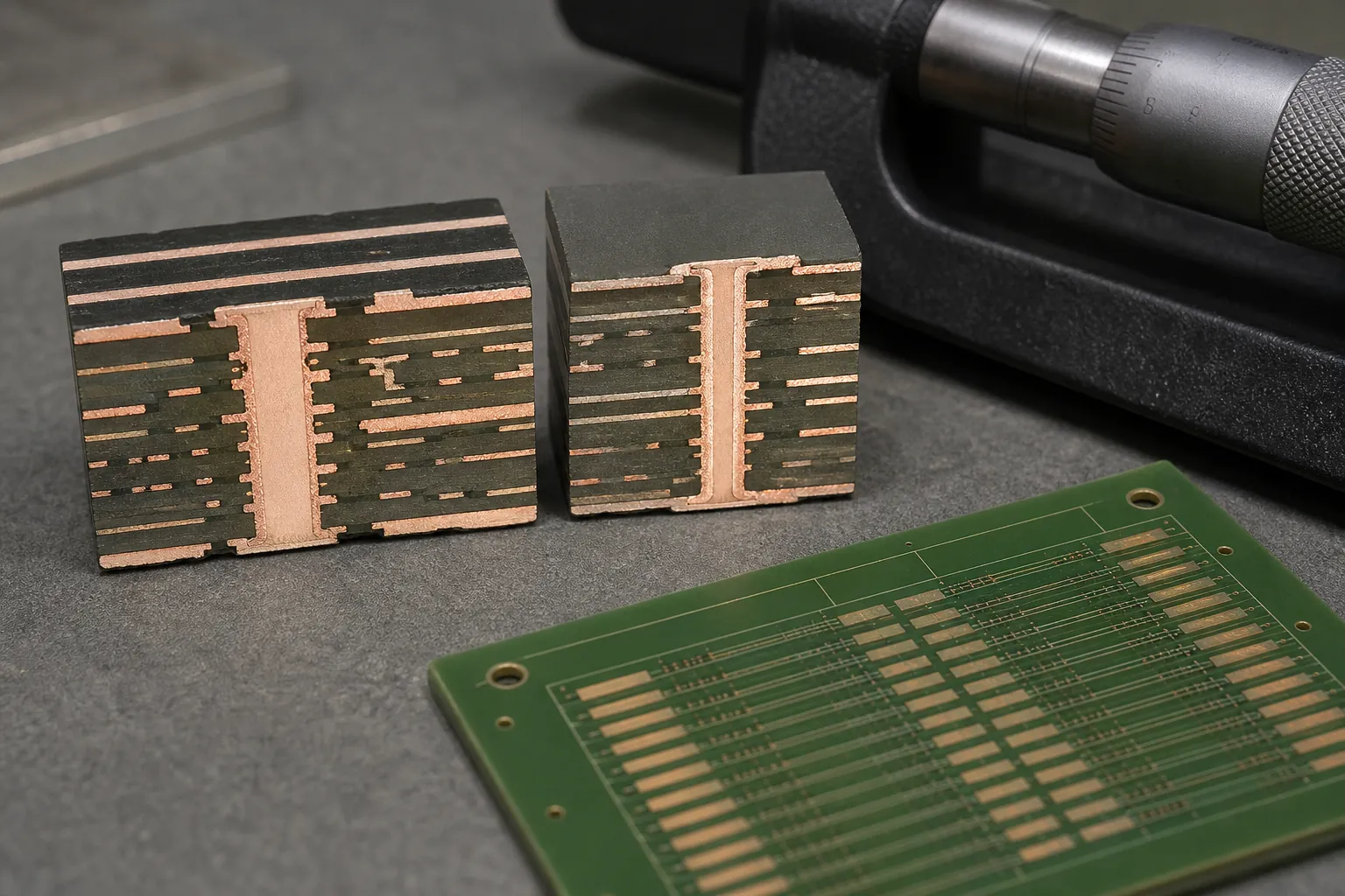
Before you accept a vendor default, review these engineering checkpoints
- Confirm which layers must carry controlled-impedance routing and what dielectric thickness the vendor default actually uses.
- Check whether each critical signal layer has a clean, continuous reference plane close enough to support return current control.
- Review copper balance across the stackup so lamination, drilling, and reflow do not introduce unnecessary warp.
- Ask whether the default stackup changes with material availability, because a quote revision can quietly move impedance and plane spacing.
- Verify that plane splits, dense via fields, and thermal relief choices still make sense once the layer order is fixed.
- Make sure assembly can tolerate the final board thickness, flatness, and thermal mass if large BGAs or bottom-terminated packages are involved.
These checks matter because a default stackup often travels from sourcing to layout to fabrication with different assumptions attached. Procurement may see a standard option. Layout sees routing freedom. Fabrication sees material pairings and press cycles. Assembly sees board flatness, heat capacity, and solder behavior. If those views are not reconciled, the “standard” decision becomes a handoff problem instead of a technical shortcut.
When the stackup should stop being standard
The stackup should stop being treated as standard when one of three things happens: the signals become sensitive enough that reference geometry drives performance, the package density forces too many compromises into one routing layer, or the fabrication and assembly process needs tighter control than the default build gives you. That might happen on a 4-layer board with awkward power conversion just as easily as on an 8-layer communications board.
Rigid-flex work is a separate case entirely. If the board bends, the stackup discussion changes from ordinary layer allocation to transition-zone stress, coverlay behavior, and bend-life management. That is why a rigid-flex stackup review should not be mixed casually with ordinary rigid-board defaults.
Choose the lowest layer count that still protects the design margins you need
A standard 2-layer PCB stackup, standard 4-layer PCB stackup, standard 6-layer PCB stackup, and 8-layer PCB stackup each have a place. The right choice is the lowest layer count that still preserves return-path integrity, routing sanity, fabrication yield, and assembly reliability without forcing repeated downstream fixes. If the default stackup meets those conditions, use it. If it does not, changing the stackup earlier is usually cheaper than debugging its consequences later.
FAQ
Is a standard 4-layer PCB stackup always better than a 2-layer stackup?
Not always. A 4-layer stackup usually gives better reference control and routing flexibility, but a simple low-speed board may not need the extra cost. The better choice is the one that meets electrical and manufacturing needs without forcing avoidable layout compromises.
When does a standard 6-layer PCB stackup become necessary?
It becomes useful when routing density, impedance control, power partitioning, or shielding needs exceed what a 4-layer arrangement can handle cleanly. Fine-pitch BGA escape, mixed noisy and sensitive sections, and faster interfaces are common triggers.
Can a vendor default stackup change from quote to quote?
Yes. Material availability, foil thickness, and process constraints can all change what a board shop considers standard. That is why controlled-impedance and plane-spacing assumptions should be reviewed again when the fabrication stackup is finalized.
Does an 8-layer PCB stackup automatically improve EMI performance?
No. Extra layers help only when the plane strategy and signal referencing are disciplined. A poor 8-layer arrangement can still create weak return paths, unnecessary transitions, and avoidable emissions problems.