What is a SOIC package?
The Small Outline Integrated Circuit (SOIC) package is a type of surface-mount IC package that is widely used in the electronics industry. It was first introduced by the electronics company Texas Instruments in 1985. The SOIC package is a rectangular plastic package with leads on two sides. The leads are bent downwards and spaced at a pitch of 1.27 mm (0.05 inches).
The SOIC package is designed to be mounted on a printed circuit board (PCB) using surface-mount technology (SMT). SMT involves soldering the leads of the package directly onto the PCB, as opposed to inserting them through holes in the board.
Development of SOIC packages
The SOIC package was developed to replace the larger Dual Inline Package (DIP) that was commonly used in the electronics industry at the time. The DIP package was bulky and required a lot of board space, which limited the number of components that could be fitted onto a PCB.
The SOIC package was designed to be smaller and more compact, allowing for more circuit board components to be fitted onto a PCB. The package was also designed to be mounted on the surface of the board, which further reduced the board space required.
SOIC Package Styles
There are several different styles of SOIC packages, each with its own unique features and specifications. The most common styles of SOIC packages are:
The narrow body SOIC package (sometimes referred to as SOx_N or SOICx_N) is a type of SOIC package that has a narrower width compared to the other two styles.
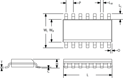
The wide body SOIC package (sometimes referred to as SOx_W or SOICx_W) is a larger version of the narrow body SOIC package, with differences mainly concentrated on the dimensions of WB and WL.
The micro SOIC package is another style of SOIC package, designed only for 8-pin or 10-pin ICs. This package is smaller than the other two styles and has a pin pitch of 0.5mm.
SOIC Package Dimensions
The dimensions of the SOIC package can vary depending on the number of pins. Here’s a table with the common SOIC package sizes and their dimensions:
| Package Size | Body Width (mm) | Body Length (mm) | Pin Count |
|---|---|---|---|
| SOIC-8 | 3.91 | 4.9 | 8 |
| SOIC-14 | 3.91 | 8.65 | 14 |
| SOIC-16 | 3.91 | 9.9 | 16 |
| SOIC-20 | 3.91 | 12.8 | 20 |
| SOIC-24 | 3.91 | 14.4 | 24 |
| SOIC-28 | 3.91 | 15.4 | 28 |

JEDEC and JEITA/EIAJ Standard
JEDEC stand for Joint Electron Device Engineering Council, while JEITA/EIAJ stand for Japan Electronics and Information Technology Industries Association / Electronic Industries Association of Japan. They are two industry organizations that develop and publish standards for electronic components, including integrated circuit packages like SOIC.
JEDEC’s standard for SOIC is MS-012, which specifies a plastic dual small outline gull wing package with a 1.27 mm pin pitch, 3.9 mm body width, and various pin counts ranging from 8 to 28.
JEITA/EIAJ’s standard for SOIC is ED-7300, which specifies a plastic small outline package with a 1.27 mm pin pitch, body widths of 5.3 mm (Type II) or 7.5 mm (Type III), and various pin counts ranging from 8 to 48.
Please note that:
- EIAJ conventionally uses SOP (5.3mm body width);
- JEDEC conventionally uses SOIC (with two body widths: 3.9mm and 7.5mm);
However, some companies do not follow these conventions, such as UTC, which uses SOP (with two body widths: 3.9mm and 7.5mm);
There are also many manufacturers that use SO, DSO, SOL, and so on.
Compare JEDEC and JEITA/EIAJ
The dimensions specified by the JEDEC and JEITA/EIAJ standards for SOP packages are different and incompatible with each other. The main differences between the two standards are reflected in the values of package width (WB) and lead width (WL). The table below shows the values of WB and WL for commonly used SOP packages according to these two standards:
| Pin Count | WB (JEDEC) | WB (EIAJ) | WL (JEDEC) | WL (EIAJ) |
|---|---|---|---|---|
| 8 | 150 mil (3.8 mm) | 208 mil (5.3 mm) | 236 mil (6.0 mm) | 310 mil (7.9 mm) |
| 14 | 150 mil (3.8 mm) | 208 mil (5.3 mm) | 236 mil (6.0 mm) | 310 mil (7.9 mm) |
| 16 | 150 mil (3.8 mm)/ 300 mil (7.5 mm) | 208 mil (5.3 mm) | 236 mil (6.0 mm)/ 400 mil (10.2 mm) | 310 mil (7.9 mm) |
| 18 | 300 mil (7.5 mm) | 208 mil (5.3 mm) | 400 mil (10.2 mm) | 310 mil (7.9 mm) |
| 20 | 300 mil (7.5 mm) | 208 mil (5.3 mm) | 400 mil (10.2 mm) | 310 mil (7.9 mm) |
| 24 | 300 mil (7.5 mm) | 208 mil (5.3 mm) | 400 mil (10.2 mm) | 310 mil (7.9 mm) |
Note: “WB” stand for width of body, “WL” stand for width of lead.
SOIC Application
- Operational amplifiers and voltage regulators. (SOIC-8)
- Timers and counters. (SOIC-14)
- Microcontrollers and memory chips. (SOIC-16)
- Analog-to-digital converters (ADCs) and digital-to-analog converters (DACs). (SOIC-20)
- Microprocessors and digital signal processors (DSPs). (SOIC-28)
SOIC Abbreviation and Meaning
| Abbreviation | Meaning |
|---|---|
| SOP | Small Outline Package |
| DSO | Dual Small Outline Package |
| SO | Small Outline |
| SOL | Small Outline L-leaded package |
| SOIC | Small Outline Integrated Circuit |
| SOW | Small Outline Package (Wide-Type) |
| SSOP | Shrink Small Outline Package |
| VSOP | Very Small Outline Package |
| VSSOP | Very Shrink Small Outline Package |
| TSOP | Thin Small Outline Package |
| TSSOP | Thin Shrink Small Outline Package |
| MSOP | Mini Small Outline Package |
| SOJ | Small Outline J-Leaded Package |
| SOT | Small Outline Transistor (sometimes called SC) |


