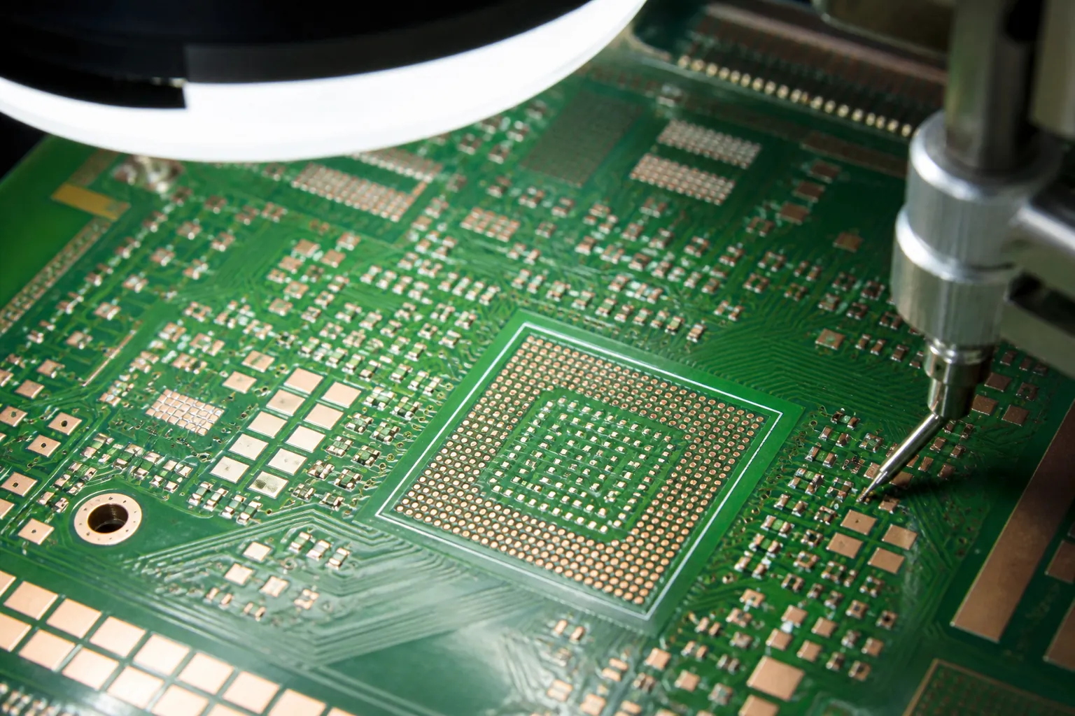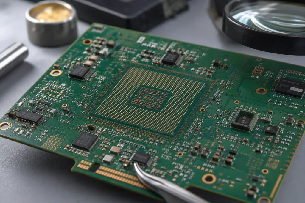
Via in pad is one of those PCB choices that looks elegant in layout view and gets expensive fast if the fabrication plan is weak. It solves real routing problems around fine-pitch BGA and dense QFN escapes, but it can also pull solder away from the joint, trap void risk under bottom-terminated parts, and add extra fill, cap, and planarization steps that not every supplier controls well. This guide explains when via in pad is worth using, what process details matter, and what design reviews should happen before you release Gerbers.
What via in pad means on a real PCB
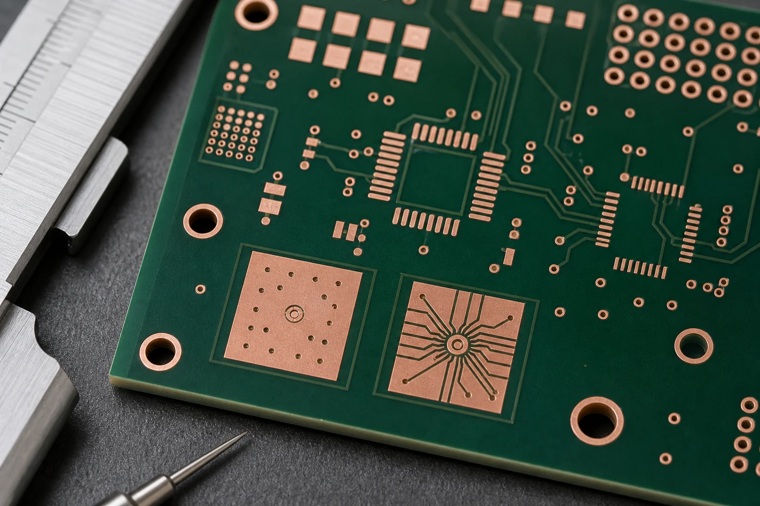
A via in pad places the drilled via directly inside the component land instead of beside it. Designers usually reach for it when the package pitch is too tight for a normal dog-bone escape, when breakout channels are limited, or when thermal and current paths need to move straight through the pad. In practice, the term often implies more than geometry. A manufacturable via-in-pad feature usually needs a defined drill strategy, copper plating target, fill method, planarized surface, and a surface finish that keeps the pad solderable.
That distinction matters because an open hole in the middle of a solderable pad behaves very differently from a filled and capped structure. The first one tends to steal solder volume and complicate inspection. The second can behave like a usable land, but only if the board shop controls fill shrinkage, copper cap quality, and final flatness tightly enough for the package you are placing.
When via in pad is the right decision
Via in pad makes sense when routing density leaves no clean alternative. Fine-pitch BGA fanout is the most common example. If the ball pitch will not support a conventional escape without collapsing trace width, violating fabrication limits, or pushing the layer count higher than the job can tolerate, a via in pad structure can unlock the layout. The same logic applies to compact RF modules, thermal pads under power packages, and HDI boards where short escape paths reduce congestion.
It can also be the better choice when a normal via beside the pad creates a different manufacturing problem. A crowded breakout can reduce solder mask dams, block rework tool access, or force awkward trace neck-downs under a component field. In those cases, a controlled via-in-pad structure may improve the whole assembly flow, not just the routing screenshot.
If your layout is still at the package planning stage, it helps to review the BGA routing rules that drive breakout choices and compare them against the stackup and supplier capability. Many via-in-pad decisions are really package-pitch decisions that surface late.
Why open via in pad causes solder and inspection trouble
The main risk is solder wicking. During reflow, molten alloy can drain into the hole or into a poorly sealed fill surface instead of staying where the joint needs volume. On a BGA, that can reduce stand-off or create hidden reliability variation from one corner of the package to another. On a QFN thermal pad, it can change void behavior and make the center paddle harder to tune with stencil design alone.
Inspection also gets harder. AOI cannot tell you much about what happened inside the via structure, and X-ray interpretation becomes more sensitive when the pad includes fill boundaries, uneven cap plating, or local voiding. Rework is not automatically easier either. If the pad surface is not flat after processing, paste release and component seating become less predictable before the board ever reaches the bench.
That is why via in pad should be reviewed together with stencil aperture strategy, paste volume, and the layout choices that affect SMT yield, inspection, and rework. The via is only one part of the joint behavior.
Filled and capped processing changes whether the idea works
A useful via-in-pad design usually needs the hole to be filled and then capped or plated over so the final pad behaves like a stable solderable surface. If the supplier offers via in pad but treats the fill step as a generic add-on, ask for specifics. The engineering question is not whether they can fill a hole in principle. The question is whether they can keep the finished pad flat enough, sealed enough, and consistent enough for your package pitch and assembly profile.
Non-conductive and conductive fills are not interchangeable
Non-conductive epoxy fill is common because it stabilizes the structure without pretending to be a low-impedance copper path. Conductive fill can be useful in specific designs, but it is not a default upgrade. Thermal behavior, coefficient-of-expansion mismatch, and final copper cap quality still matter more than the sales label on the fill material. For many boards, the decisive requirement is not conductivity through the fill but a sealed, planar pad that will not starve the joint during reflow.
Planarity is a release criterion, not a cosmetic detail
If the capped surface sinks, domes, or leaves edge texture, the defect shows up later as poor paste print, inconsistent collapse, or unreliable contact under bottom-terminated parts. That is why procurement, fabrication engineering, and assembly should align early on what finished pad flatness is acceptable. A via-in-pad feature that passes bare-board electrical test can still be the wrong choice for assembly yield.
Layout checkpoints before you release Gerbers
Do not release via in pad based only on DRC clearance. Review the pad stack, drill size, aspect ratio, fill note, cap requirement, and paste strategy as one package. On BGA escapes, confirm that the breakout gain is real enough to justify the process cost. On thermal pads, confirm whether segmented paste apertures and the via field work together instead of fighting each other.
- Check whether the package pitch truly blocks a conventional escape route.
- Confirm the board shop’s via fill and planarization capability for the actual hole size, not a generic capability sheet.
- Review solder mask behavior around the pad so adjacent dams and paste release stay manufacturable.
- Ask assembly whether stencil thickness, aperture reductions, or windowpane patterns need to change.
- Flag any pads that will rely on X-ray because optical inspection will be weak after placement.
- Verify whether repair or component replacement is realistic if the part ever has to come off the board.
For designs already moving toward high-density interconnect, the HDI PCB guide and the broader PCB via overview are useful references for deciding whether a microvia build-up path is cleaner than forcing every dense problem into one via-in-pad rule.
When a conventional escape is usually better
Via in pad is not a badge of design maturity. If the package pitch is manageable, board area is available, and a dog-bone or nearby via meets routing goals without driving layer count or signal integrity problems, the simpler structure is often the better production choice. It is easier to inspect, cheaper to fabricate, and less sensitive to fill-quality variation.
This is especially true on cost-sensitive builds, serviceable industrial controls, and products that may need field replacement of expensive ICs. A layout that looks slightly less compact but keeps the solder joint conventional can save time in first article inspection, X-ray review, and rework training. That tradeoff matters more than aesthetic neatness.
Cost and lead-time questions buyers should ask early
Via in pad often changes both quote quality and schedule risk. The extra fabrication steps can narrow the pool of acceptable suppliers, and the real risk is not only unit cost. It is late-stage discovery that the chosen shop fills the hole one way while assembly expected another. Buyers and program managers should ask whether fill, cap, planarization, and any inspection hold points are included in the quote assumptions. If they are missing, the first NPI batch can drift into a re-spin argument about responsibility instead of yield.
A short clarification list early in sourcing usually prevents the worst surprises: which via sizes can be filled reliably, whether conductive or non-conductive fill is being quoted, what flatness standard the supplier uses internally, and whether sample coupons or X-ray evidence are available on first article builds. Those are practical purchasing questions, not paperwork overhead.
Use via in pad when the package demands it, not because it sounds advanced
Via in pad is valuable when it solves a real escape, thermal, or density problem that ordinary routing cannot handle cleanly. It becomes risky when teams treat it as a default shortcut and skip the fill, cap, paste, and inspection conversation. If the board shop, assembler, and layout owner agree on the finished pad behavior before release, via in pad can support reliable dense assemblies. If they do not, the same feature can turn into a silent yield drain that only shows up under X-ray or during rework.
FAQ
Does via in pad always need to be filled?
For most assembly-critical pads, yes. Leaving the hole open usually increases solder wicking risk and makes the finished pad less predictable during reflow. The exact fill and cap method depends on package pitch, hole size, and supplier capability, but an unfilled via in a solderable pad is rarely the safe default.
Is via in pad the same as using a microvia under a BGA?
Not exactly. A microvia can be part of a via-in-pad strategy, but via in pad describes the via location relative to the pad, not the via type by itself. Some designs use laser microvias in pad on HDI builds, while others use mechanically drilled structures that then require fill and planarization.
Why does via in pad increase PCB cost?
It usually adds process steps such as fill, cure, planarization, copper cap work, and tighter process control during fabrication and inspection. It can also narrow supplier choice and increase NPI review time because assembly and bare-board requirements are more tightly coupled than with a conventional escape.
When should a designer avoid via in pad?
Avoid it when a conventional nearby via meets routing needs without forcing trace or layer compromises, or when the build is highly cost-sensitive and serviceability matters more than extreme density. If the package pitch does not demand it, the simpler land pattern is often easier to fabricate, inspect, and rework.