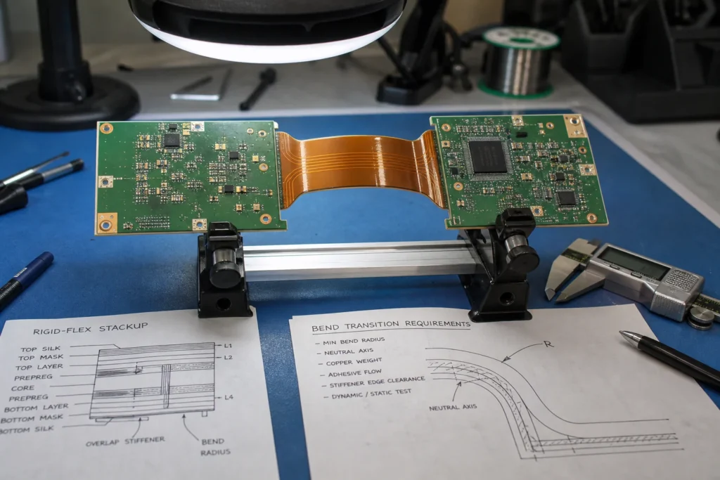
A rigid-flex PCB stackup is usually decided before anyone sees a cracked trace, lifted pad, or unstable impedance result. That is exactly why it matters. Once the layer order, copper weight, adhesive system, stiffener plan, and bend-zone rules are frozen, most of the later reliability outcomes are already constrained. If the stackup is wrong, no amount of careful assembly will fully rescue it.
This guide focuses on the practical engineering decisions behind a rigid-flex PCB stackup: what belongs in the bend area, what should stay out, how transitions fail, and how to balance flexibility with manufacturable impedance control. If you are choosing between rigid and flex constructions, or trying to stop field failures near a fold line, these are the checkpoints that matter.
What a rigid-flex PCB stackup actually has to control
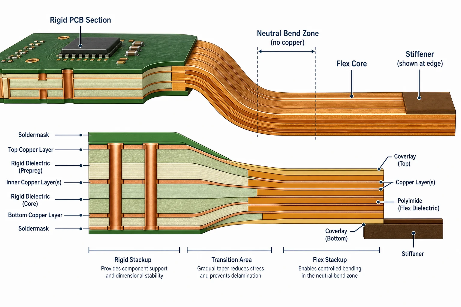
A useful rigid-flex stackup does four jobs at the same time. It has to survive mechanical bending, maintain electrical performance, stay buildable at the fabricator, and remain inspectable and assembly-safe at the transitions between rigid and flex regions.
That is why a stackup decision cannot stop at “two rigid sections plus one flex core.” The engineer still has to define copper distribution, dielectric thickness, adhesive or adhesiveless material choice, coverlay behavior, shield or ground usage in the flex, and where stiffeners start and stop. Each of those choices affects more than one failure mode.
Start with the bend region, not the rigid region
Many teams begin the stackup discussion around the rigid part of the board because that is where most components, BGA fanout, and controlled-impedance routing live. In rigid-flex work, that is backwards. The bend area is the hardest part to recover later, so it should drive the first stackup decisions.
If the flex section must move repeatedly, the copper needs low strain, balanced placement, and clean neutral-axis behavior. If it only folds once during installation, the stackup can tolerate more copper and shielding, but the fold radius and transition anchoring still need definition. The required bend life changes the acceptable copper thickness, layer count in the flex, and whether traces can cross the bend on multiple layers.
Bend-life questions to settle early
Before you approve a rigid-flex stackup, answer these questions explicitly rather than burying them in fab notes.
- Is the flex dynamic, limited-cycle, or install-once only?
- What bend radius is physically available in the product enclosure?
- Will the bend sit near a connector, stiffener edge, or heavy copper transition?
- Does the flex section carry high-speed pairs, power, or only low-risk control signals?
- Will the product see thermal cycling that changes stiffness at the transition?
When these answers are vague, the stackup often becomes overbuilt in the wrong places and under-protected in the places that actually crack first.
Why copper symmetry matters more than people expect
Rigid-flex failures often begin because the copper distribution through the flex is mechanically unbalanced. One layer may carry a dense reference plane while the opposite side has sparse routing. That shifts the neutral axis and concentrates strain where the copper already has stress risers at pads, teardrops, and etched corners.
In practice, balanced copper does not always mean identical artwork. It means the stackup and routing strategy should avoid putting one side of the flex into a much harsher strain condition than the other. Designers sometimes fixate on impedance targets and forget that a flex pair routed beside a large copper pour on only one side can pass simulation yet still fail bend cycling.
That tradeoff is especially important when a rigid-flex PCB stackup includes shielding layers. A full copper shield may improve EMI, but if it forces asymmetric strain in the bend area, the mechanical cost can outweigh the electrical benefit.
Coverlay, adhesive systems, and stiffeners are part of the stackup decision
Engineers often discuss stackup as if it ends at copper and dielectric. In rigid-flex boards, coverlay and stiffener details belong in the same conversation because they directly affect both manufacturability and fatigue life.
Coverlay openings that are too aggressive can create stress concentration near pad exits. Adhesive-based constructions may behave differently from adhesiveless materials during heat exposure and repeated flexing. Stiffeners improve local support for connectors and components, but a poorly placed stiffener edge can create a hinge effect that concentrates stress right where traces leave the rigid support.
Typical transition-zone mistakes
- Ending a stiffener exactly where dense traces enter the flex.
- Placing vias or pad arrays too close to the rigid-to-flex boundary.
- Using heavy copper in a bend section simply because the rigid area needs it.
- Assuming coverlay openings can follow rigid-board solder mask habits.
These are not cosmetic issues. They influence crack initiation, peel risk, and solder-joint fatigue once the assembly is bent, handled, or thermally cycled. The same handling discipline also affects flex PCB assembly handling and reliability after fabrication.
Controlled impedance in a rigid-flex stackup needs a location-specific mindset
Impedance control inside rigid-flex boards is usually harder at the handoff than inside the stable rigid area. The dielectric environment, copper reference conditions, and manufacturing tolerances can change across the structure. That means a trace pair that behaves predictably in the rigid section may see different coupling or reference continuity as it approaches the flex transition.
If high-speed signals must cross the flex, the stackup should be planned with a clear return-path strategy and with realistic geometry that the fabricator can actually hold. This is one reason a generic “recommended flex stackup” from an old reference article is rarely enough. If you need a baseline refresher on PCB stackup design basics, use it as a starting point, then adapt the details to rigid-flex stress and transition behavior. The mechanical function of the flex and the electrical function of the signals need to be solved together.
When the signal budget is tight, it is often better to keep the bend area electrically simple and move the hardest routing back into the rigid sections. That may mean reserving the flex for a smaller set of signals, widening the bend radius, or accepting a different connector position so the transition is less electrically abrupt.
What to keep out of the bend area
The cleanest rigid-flex layouts treat the bend zone as a protected mechanical feature, not spare routing real estate. That usually means avoiding plated through-holes, stacked vias, abrupt plane splits, large pads, and concentrated copper islands in the section expected to flex.
It also means keeping silkscreen, adhesive discontinuities, and unsupported component weight away from the area that has to move. Even when a design survives electrical test, these details can shorten bend life in the field or create intermittent faults that are hard to reproduce on the bench.
Good bend-zone discipline usually includes
- Routing traces perpendicular to the bend when possible.
- Staggering traces rather than packing them into one strain line.
- Using rounded trace geometry and smooth neck-down transitions.
- Keeping copper away from the absolute outer edge of repeated-bend regions.
- Reserving the bend for the minimum signal set needed.
If the mechanical team cannot provide enough bend radius, the right answer may be to change the enclosure or harness strategy instead of forcing a stackup that only looks acceptable in CAD.
DFM review should happen before the stackup is treated as final
A rigid-flex PCB stackup can look reasonable in an internal design review and still create supplier-side friction. Fabricators need to know whether the construction relies on specific polyimide thicknesses, whether coverlay registration is tight, whether impedance coupons are needed, and how the rigid and flex lamination sequence will be built. Assemblers need to know how the panel will be supported, whether temporary carriers are required, and where handling damage is most likely.
That is why the stackup review should include fabrication and assembly questions, not only ECAD signoff. If the board needs a carrier for SMT, the carrier strategy can affect fiducial access, underside clearance, and reflow shadowing. If the flex tail folds near a connector, inspection access and final functional test fixtures may also need changes.
These are classic DFM and DFT consequences: the stackup choice changes not just reliability, but how the board is built, inspected, and debugged.
How to compare a rigid-flex stackup against a simpler flex-only stackup
Some designs are labeled rigid-flex when they are really flex assemblies with local reinforcement. Others truly need multiple rigid islands connected through flex for packaging and signal-routing reasons. A broader Rigid-Flex PCB overview helps frame where that architecture makes sense before the stackup details are frozen. The distinction matters because rigid-flex brings lamination complexity, transition-risk management, and higher process sensitivity.
If the product only needs a short folded interconnect with modest component density, a simpler flex circuit plus stiffeners may be enough. If the design needs dense components on multiple rigid sections with a controlled fold path between them, rigid-flex becomes easier to justify. The stackup decision should follow that product architecture, not habit.
A practical review question is this: what problem does the rigid-flex stackup solve that separate rigid boards and a cable cannot solve cleanly? If the answer is not specific, the design may be carrying unnecessary manufacturing risk.
Before release, verify the stackup against real failure checkpoints
Before release, review the stackup with failure analysis in mind rather than treating the fab drawing as the finish line.
- Check whether copper thickness in the flex matches the required bend life.
- Confirm the rigid-to-flex transition does not place vias, pad exits, or stiffener edges in the highest-strain zone.
- Verify that impedance-critical nets keep a stable reference strategy across the transition.
- Review coverlay openings for peel risk and registration tolerance, not only pad access.
- Make sure assembly fixtures, carriers, and test access still work with the folded geometry.
Those checkpoints catch the kinds of issues that otherwise show up later as cracked conductors, noisy links, intermittent opens, or expensive NPI rework.
Conclusion
A rigid-flex PCB stackup is not successful because it fits into the enclosure or passes one impedance table. It is successful when the flex survives its real bend duty, the transition zones stay crack-resistant, the assembly process remains controllable, and the electrical behavior is stable where it matters. That requires the stackup to be treated as a mechanical, electrical, and manufacturing decision at the same time.
If you are building a rigid-flex design, the safest approach is to define the bend requirement first, simplify the flex region aggressively, and review every transition as a likely failure origin. That is how a rigid flex PCB stackup becomes a reliability tool instead of a future debug problem.
FAQ
What is the most important factor in a rigid-flex PCB stackup?
The most important factor is the real mechanical duty of the flex region. If the board will bend repeatedly, copper weight, layer symmetry, bend radius, and transition support matter more than a generic layer recipe.
Can controlled-impedance signals cross a rigid-flex bend area?
Yes, but only when the stackup, return path, and geometry are planned for that transition. Many teams keep the bend area electrically simpler because mechanical reliability and impedance control can conflict in a tight flex section.
Why do rigid-flex boards often fail near the transition instead of the middle of the flex?
The transition is where stiffness changes, copper routing gets denser, and stiffeners or pads often end. That combination concentrates stress, so cracks and intermittent opens often start there first.
Should a rigid-flex stackup include heavy copper in the flex section?
Usually only when the electrical requirement clearly justifies it. Heavier copper increases strain during bending, so it can shorten flex life if it is carried through a dynamic or limited-cycle bend region without a strong reason.