A transimpedance amplifier looks simple on paper: a current source, an op-amp, a feedback resistor, and often a small feedback capacitor. In production hardware, that simplicity is deceptive. The stage is usually handling a tiny sensor current, sitting next to input capacitance that moves the loop phase, and sharing a PCB with supplies, clocks, cables, or LED drivers that inject unwanted energy into the most sensitive node on the board.
That is why many transimpedance amplifier problems do not show up as obvious design mistakes. The board powers up, the sensor responds, and the output even looks correct at one light level or one gain setting. Then the signal gets noisy, recovery becomes slow after overload, or the front end starts ringing when a cable length changes. For engineers building photodiode receivers, optical sensors, or other current-output measurement chains, the practical question is not just what a transimpedance amplifier does. The real question is how to make one stay stable, quiet, and testable on a real PCB.
This guide takes that practical angle. Instead of repeating a textbook definition, it focuses on the design decisions that usually determine whether a transimpedance stage becomes a reliable measurement front end or a recurring debug problem. If you already work through PCB schematic design practices carefully, this is the next level where component choice, feedback compensation, and layout discipline start to matter more than block-diagram correctness.
What a transimpedance amplifier is really doing
A transimpedance amplifier converts input current into output voltage. In sensor work, that current often comes from a photodiode, but the same idea shows up anywhere the source behaves more naturally as a current than as a low-impedance voltage. The feedback resistor sets the basic current-to-voltage gain, so a larger resistor gives more volts per ampere. That sounds straightforward until the rest of the system enters the picture.
The input source is rarely ideal. A photodiode brings junction capacitance. The op-amp adds input capacitance and finite gain-bandwidth. PCB pads, traces, and cables add more capacitance. All of that appears around the inverting node, which is exactly where a transimpedance amplifier is most sensitive. The feedback capacitor is not an optional decoration in many designs; it is often the part that keeps the circuit from overshoot, peaking, or outright oscillation.
In other words, a transimpedance amplifier is less like a generic op-amp gain block and more like a carefully balanced sensor interface. If the front end also feeds comparators, ADCs, or digital processing, the output behavior must support the rest of the signal chain. That is where understanding analog and digital signals helps: the amplifier is not judged only by gain, but by bandwidth, noise floor, settling behavior, and how cleanly it hands the signal to the next stage.
Why general op-amp habits often fail in transimpedance circuits
Input capacitance changes the loop faster than most engineers expect
A non-inverting voltage amplifier can tolerate layout laziness that a transimpedance stage cannot. In a TIA, the inverting node is effectively a summing junction with very high sensitivity to capacitance. Every extra pad, long trace, or connector stub can shift stability margin. A circuit that looks fine in simulation with idealized values may ring or peak once the real sensor package and board parasitics are present.
Higher gain is not free gain
Large feedback resistance increases conversion gain, but it also increases Johnson noise and often forces a narrower practical bandwidth. If the application needs both high sensitivity and useful speed, resistor value alone will not solve the problem. The op-amp, sensor capacitance, compensation capacitor, and expected light or current range must be chosen together.
Recovery from overload can dominate real performance
In optical or instrumentation systems, the hardest moment may not be steady-state measurement. It may be what happens when the sensor sees a burst, an ambient-light step, or a current surge that pushes the amplifier near a rail. Some parts recover gracefully. Others take too long to come back, leaving the downstream ADC or comparator blind during the interval that matters most. Engineers sometimes blame the sensor when the real issue is overload behavior in the front end.
Choosing the feedback resistor and capacitor from system targets
Start with the measurement objective, not the resistor drawer. Ask four questions first: what current range must be resolved, what output range the next stage wants, what bandwidth is truly needed, and what sensor capacitance you are carrying at the input. Those answers define the useful design window.
The feedback resistor normally comes from the output swing you want at the expected current level. If your target current is small and your ADC needs meaningful amplitude, the resistor may need to be large. That raises noise and increases the need for careful compensation. If the signal changes quickly, the resistor may need to come down so the stage can settle and remain stable with available op-amp bandwidth.
The feedback capacitor is the part that many first-pass designs underestimate. In practice, it is there to shape loop response against total input capacitance. Too little capacitance and the stage can peak or oscillate. Too much and bandwidth collapses unnecessarily. The right value comes from the combination of op-amp gain-bandwidth, sensor capacitance, and the feedback resistor you chose for transimpedance gain. That is why TIAs reward iterative bench tuning much more than formula-only confidence.
A good workflow is to calculate a sane starting range, simulate with realistic source capacitance, then verify on hardware with the actual sensor or a close capacitance equivalent. If your measurement front end will ever see alternate sensor lots, long leads, or connector options, include those variants in the validation plan before release.
PCB layout rules that matter more than another decimal place in the datasheet
Keep the input node physically small
The shortest trace on the board should often be the connection from the sensor to the inverting input. Do not route it like an ordinary signal. Avoid unnecessary test pads, long meanders, or adjacency to switching nodes. If the sensor package allows it, place the photodiode or current source as close to the op-amp input as the mechanical design permits.
Place the feedback network directly around the op-amp
The feedback resistor and capacitor should sit tightly around the amplifier pins, not off in a convenient open area. A long feedback path adds inductance and collects noise. On a TIA board, the feedback loop is part of the control system, so treating it like a casual route usually costs stability margin.

Give the front end a clean return path and local decoupling
A quiet signal node still fails if the amplifier supply is dirty. Put local decoupling close to the op-amp supply pins, keep return currents predictable, and separate the sensitive analog region from fast digital activity when possible. If the board also carries clocks, switching regulators, or LED drivers, think about current return paths, not just component placement labels.
Use shielding and guarding only when they solve a specific problem
Guard rings, shields, and grounded copper can help with leakage and noise pickup, but they are not magic decorations. Use them deliberately around very high-impedance nodes or where leakage paths are credible. If the issue is actually poor compensation or a bad return path, decorative guarding will not rescue the design.
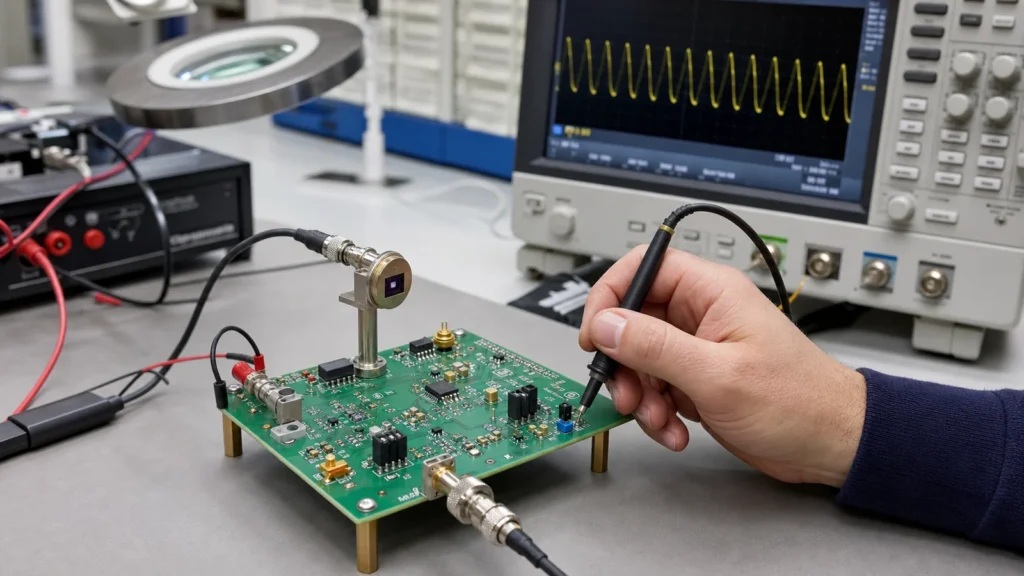
Bench checks that catch most TIA mistakes before a redesign
When a transimpedance amplifier misbehaves, do not start by swapping op-amps blindly. First isolate the failure mode. Is the issue oscillation, noise, overload recovery, bandwidth loss, or gain error? The bench setup should answer that directly.
Start with a controlled input condition. If the real sensor is inconvenient, substitute a known current source or at least a repeatable test arrangement. Then check the output for peaking, ringing, or slow settling while changing light level, modulation frequency, or source capacitance. If adding cable length or touching the input area changes the waveform noticeably, layout and input parasitics are already telling you where the weakness is.
Also verify the supplies under load and inspect the output at the operating points that matter most, not just at the comfortable midpoint. Many front ends look acceptable at one condition and fail near the limits. A useful discipline is to document these measurements the same way you would document any other mixed-signal review, so the schematic and bench evidence remain aligned when the design comes back for revision. That makes later debug work much easier when someone else has to read electrical schematics and retrace the original intent.
When a transimpedance amplifier may not be the right answer
Not every sensor current problem wants a classic TIA. If the source current is large, speed is modest, and dynamic range is forgiving, a simpler resistor-based approach may be acceptable. If the required bandwidth and noise targets are both aggressive, a staged architecture or specialized front-end IC may be easier to control than a one-op-amp solution. The right choice depends on whether the front end is acting as a precision instrument, a detection threshold stage, or a general-purpose sensor input.
The key engineering mistake is treating the transimpedance amplifier as default rather than justified. Use it when current-to-voltage conversion with controlled gain, speed, and noise actually serves the system goal. Then design the PCB as part of the amplifier, not as a neutral container around it.
Conclusion
A transimpedance amplifier earns its reputation by solving a real measurement problem, but it only keeps that reputation when the sensor, op-amp, compensation, and PCB layout are treated as one system. The failure modes are usually subtle: a little extra capacitance, a feedback loop placed too far away, a gain target chosen without recovery behavior in mind. Those details are exactly what decide whether the board becomes stable test hardware or a noisy front end that only works on the bench one day out of five.
If your design review is approaching, the most useful mindset is simple: shrink the sensitive node, place the feedback network tightly, choose gain from system needs, and validate stability with the real source capacitance. That approach will do more for transimpedance amplifier performance than another round of generic op-amp swapping.
Why does a transimpedance amplifier usually need a feedback capacitor?
A feedback capacitor helps stabilize the loop against total input capacitance from the sensor, op-amp input, PCB pads, and cables. Without enough compensation, the stage can peak, ring, or oscillate even when the resistor value looks correct for gain.
Can I use any fast op-amp as a transimpedance amplifier?
No. A fast op-amp is not automatically a good TIA choice. Input capacitance, input bias current, gain-bandwidth behavior, overload recovery, noise, and how the part behaves with your source capacitance all matter. A part that works well in a voltage-gain stage can still behave poorly in a photodiode front end.
How close should the photodiode be to the amplifier input on the PCB?
As close as your mechanical design allows. The sensor-to-inverting-input connection should usually be one of the shortest and quietest routes on the board because extra trace length adds capacitance and increases noise pickup at the most sensitive node in the circuit.
Why does the output recover slowly after a bright-light or current overload event?
The amplifier may be saturating or operating with compensation and gain choices that make overload recovery slow. In many real systems, overload behavior is a major performance limit, so recovery should be checked on the bench rather than assumed from small-signal calculations.