What is an integrated circuit?
An integrated circuit (IC) is an electronic circuit built on a single semiconductor chip. It is the most commonly used form of electronic device in computers, mobile phones, and other electronics. Generally, an IC is a small piece of silicon, about one-eighth of an inch square, that contains thousands or millions of transistors, resistors, and other circuit board components. This type of miniature circuitry allows for a variety of functions to be performed at a much smaller size and with greater efficiency than if the components were constructed separately.
Components of an integrated circuit
Integrated circuits are made up of several components, each of which performs a specific function. These components are typically connected together by tiny metal traces, which are used to carry electrical signals between the various parts of the circuit. The components are usually very small, ranging from a few micrometers to a few millimeters in size. This allows for a large number of components to be placed on a single chip, allowing for a greater degree of complexity and functionality.
Benefits of integrated circuits
Integrated circuits are powerful tools that allow us to increase the complexity and functionality of our electronics. By placing multiple components onto a single chip, we can reduce the amount of space required for a device. This, in turn, reduces costs and increases the efficiency of the device. The integration of components also helps to reduce electromagnetic interference, enabling our electronics to work more reliably. Integrated circuits are the foundation of modern electronics and are essential to our daily lives.
Applications of integrated circuits
Integrated circuits are the basis for most modern electronics. They are used in computers, mobile phones, TVs, radios, and many other electronic devices. They can also be found in appliances such as washing machines, microwaves, and dishwashers. In addition, they are increasingly being used in medical devices, industrial machinery, and automotive systems.
IC Design Process Overview
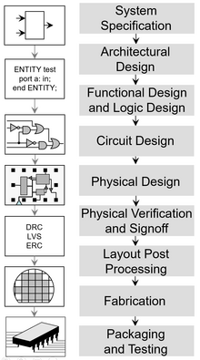
IC design is a complex process for designing electronic circuits. It involves several steps, including front-end design, back-end design, and final assembly. The process is highly iterative and requires close collaboration between the designer and the engineers to ensure that the design meets all of the required specifications. At each step of the process, prototypes are created to test and verify that the designs are working as expected.

Front-end design
Front-end design of integrated circuits is the process of designing the basic components of an integrated circuit (IC), such as transistors, resistors, and capacitors. This is done using a variety of tools, such as schematic capture, logic synthesis, and layout software. The goal of front-end design is to create an IC that meets the desired specifications.
IC Specifications
The IC specifications of IC design define the core components and attributes that the circuit must incorporate. It is the foundation upon which the entire design process will be built. The specifications should be able to capture all of the requirements needed to create a successful IC design. Furthermore, it must be able to adapt to the changing needs and technologies of the industry. The correct IC specifications are crucial for an efficient and effective design process, so it is important to ensure they are properly established to ensure success.
Detailed design
Fabless comes up with a design solution and a specific implementation architecture according to the specification requirements put forward by the customer, and divides the module functions.
HDL coding
HDL is a powerful hardware description language for IC design. It provides an efficient means of describing complex designs and allows for early validation of the functionality of the design. HDL is widely used in industry, making it an essential technology for modern IC designers. The flexibility and scalability of HDL makes it advantageous for use in a variety of applications and on multiple platforms. This enables designers to develop efficient and comprehensive IC designs that are well-suited for their specific needs. HDL is a critical tool in the success of any IC design project and its use should be strongly considered by any designer looking to create a successful integrated circuit.
Simulation verification
Simulation verification is an essential step in the IC design process. It helps designers to identify any potential errors and design flaws during the development phase. This process involves running simulations and tests on the IC designs to ensure that they meet the required specifications and standards. Simulation verification is useful for detecting bugs, resolving design issues, and optimizing the performance of the IC design. Furthermore, it allows designers to better understand how their IC designs will behave in real-world conditions. Therefore, simulation verification plays an important role in ensuring the reliability of IC designs before they are deployed in production.
(simulation verification tool: Synopsys’ VCS , and Cadence’s NC-Verilog.)
Logic synthesis——Design Compiler
Simulation verification is passed, and logic synthesis is carried out. The result of logic synthesis is to translate the designed and implemented HDL code into a gate-level netlist netlist. Synthesis needs to set constraints, which are the standards you want the synthesized circuit to meet in terms of target parameters such as area and timing. Logic synthesis needs to be based on a specific comprehensive library. In different libraries, the area of the basic standard cell (standard cell) of the gate circuit and the timing parameters are different.
Therefore, the selected comprehensive libraries are different, and the synthesized circuits are different in timing and area. Generally speaking, after the synthesis is completed, simulation verification needs to be done again (this is also called post-simulation, and the previous one is called pre-simulation).
(Logic synthesis tool: Synopsys’ Design Compiler)
STA
STA, is mean static timing analysis, which also belongs to the verification category, it mainly verifies the circuit in terms of timing, and checks whether the circuit has violations of setup time and hold time (violation). This is the basic knowledge of digital circuits. When these two timing violations occur in a register, there is no way to correctly sample data and output data, so there will definitely be problems with the function of digital chips based on registers.
(The STA tool: Prime Time of Synopsys.)
Formal verification
This is also the verification category, which is to verify the synthesized netlist from the function (STA is timing). The most commonly used method is the equivalence checking method. With the HDL design after functional verification as a reference, compare the netlist functions after synthesis to see if they are functionally equivalent. This is done to ensure that the circuit function described by the original HDL has not been changed during the logic synthesis process.
(The formal verification tool: Synopsys Formality.)
Back-end design
Back-end design of integrated circuits is the stage of the design process where the physical layout of the circuit is created. This includes designing the metal masks, routing the metal layers, and other physical aspects of the circuit. The back-end design is often the longest and most detailed part of the design process, and is critical for ensuring that the circuit works correctly. This can also involve advanced techniques like using Redistribution Layers (RDL) for optimized connectivity.
DFT
Design For Test, design for testability. Chips often have built-in test circuits, and the purpose of DFT is to consider future tests during design. A common approach to DFT is to insert scan chains into the design to turn non-scanning units (such as registers) into scanning units. Regarding DFT, there are detailed introductions in some books, so it is easier to understand it by comparing it with pictures.
(DFT tool: Synopsys’ DFT Compiler)
Floorplan
Floorplan is to place the macrocell module of the chip, and generally determine the placement of various functional circuits, such as IP modules, RAM, I/O pins, and so on. Floor planning can directly affect the final area of the chip.
(The Floorplan tools: Synopsys’ Astro)
CTS
Clock Tree Synthesis, clock tree synthesis, simply put, it is the wiring of the clock. Due to the global command function of the clock signal in the digital chip, its distribution should be symmetrically connected to each register unit, so that when the clock reaches each register from the same clock source, the clock delay difference is the smallest. This is also why the clock signals need to be routed separately.
(The CTS tool: Physical Compiler of Synopsys.)
Layout & Route
The route here is ordinary signal wiring, including wiring between various standard units (basic logic gate circuits). For example, the 0.13um process we usually hear, or the 90nm process, is actually the minimum width that the metal wiring can achieve here, and it is the channel length of the MOS tube from a microscopic point of view.
(The routing tool: Astro from Synopsys)
Parasitic extraction
Parasitic extraction of IC design is an important process in the development of integrated circuits. It is a process of extracting parasitic elements such as capacitance, inductance and resistance from the physical layout of the circuit. This process is critical to ensure that the IC design meets the performance requirements desired by the user. The accuracy of the parasitic extraction also plays a key role in ensuring that the design behaves as expected. Overall, parasitic extraction of IC design is a crucial step in achieving good operational performance from an integrated circuit.
(Parasitic extraction tool: Synopsys Star-RCXT)
Physical Verification
Physical verification of integrated circuit layout design is a crucial step in the process of IC design. It occurs after the schematic design and typically involves the use of LVS (Layout vs Schematic) verification, DRC (Design Rule Checker), and ERC (Electrical Rule Checker). LVS verification verifies that the physical layout matches the schematic design. DRC checks for violations of design rules that are set by the fabrication process while ERC checks for electrical errors. All these checks are important to make sure that the design is correct and ready to be fabricated. Physical verification helps to ensure that the IC design meets the desired specifications and requirements.
(The Physical verification tool: Hercules from Synopsys)
The completion of the physical layout verification means that the entire chip design phase is completed, and the following is the chip manufacturing.
IC Designing Tips and Tricks
– Understand the project requirement in detail.
– Break down the design into blocks and assign tasks.
– Analyse the power requirements and choose the correct devices.
– Design the circuit carefully keeping the design rules in mind.
– Validate the design with simulations.
– Debug the design and perform layout optimization.
– Generate GDS and validate the design in the target board.
– Use power estimation and optimization techniques.
– Choose the right components.
– Consider timing and power constraints.
– Make use of design automation tools.
– Perform verification and design debug.
– Take advantage of advanced IC design tools.
– Use hierarchical design for complex designs.
– Be mindful of power, area and performance tradeoffs.
– Design for testability and debugability.
– Create a comprehensive design documentation.


