
SOIC Packages: Design & Soldering Guide
SOIC small-outline ICs: pin spacing, thermal management, and SMT assembly tips. Compare with DIP for compact PCB designs. Best practices inside!
SOIC small-outline ICs: pin spacing, thermal management, and SMT assembly tips. Compare with DIP for compact PCB designs. Best practices inside!
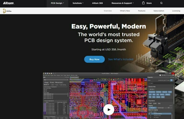
Top PCB design tools: Altium, KiCad, Eagle, and more. Features, pricing, and user reviews for engineers. Compare free vs paid options.
PCB designers need to understand PCB trace basics to create high-performance printed circuit boards. From basic definitions to the types of traces, this article covers all the fundamentals you need. Working with printed circuit board (PCB) design software can be
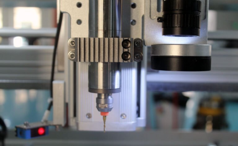
PCB cutting can make or break your electronics project. Whether you’re crafting a one-of-a-kind prototype or preparing for mass production, getting it right is essential. But with so many tools and techniques available, where do you start? This comprehensive guide
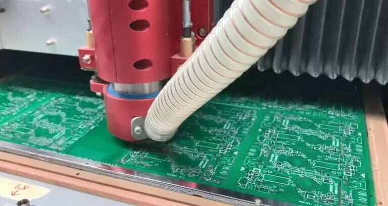
We have advanced equipment to support rapid PCB prototyping. Depending on the situation, the entire production process takes about one to three weeks. The prototype is first tested in the laboratory, and we will send the test report to the

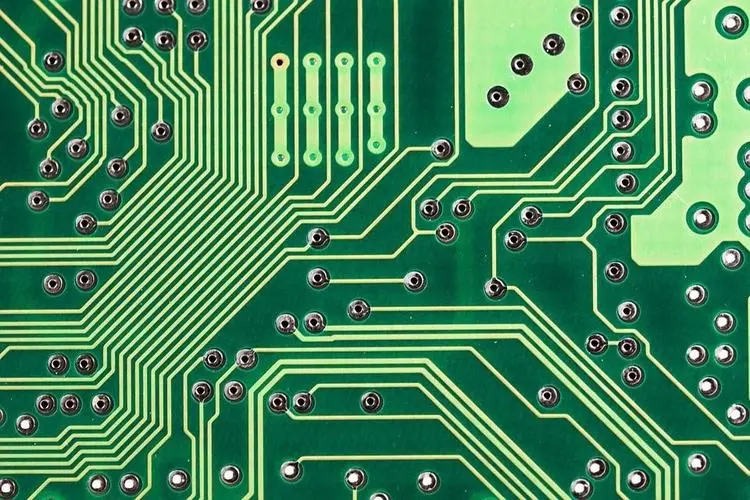
What is PCB Footprint? PCB footprint, is the arrangement of pads used to mount a specific component to a printed circuit board. The footprint defines the outline of the component and the location of the mounting pads. It’s an important

Master PCB BOM creation: component listing, part numbers, and sourcing. Tips for accuracy, cost optimization, and manufacturability. Download template inside!

Choose PCB connectors: pin headers, FPC, and circular types. Tips for durability, current rating, and layout. Critical for reliable system integration. Guide inside!
Imagine building a city’s subway system blindfolded. That’s what designing a modern printed circuit board (PCB) often feels like—threading microscopic pathways for electricity while juggling heat, signal interference, and space constraints. Now, artificial intelligence is lifting that blindfold. As DeepSeek’s
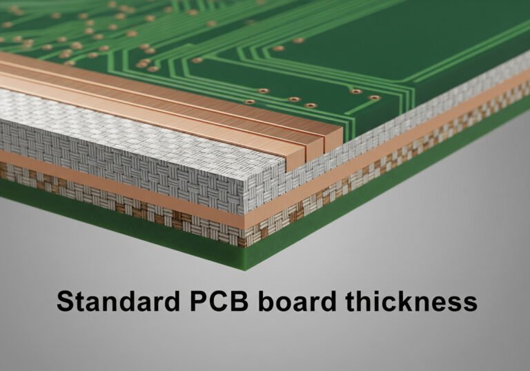
A comprehensive guide to standard PCB board thickness. Learn its impact on mechanical stability & electrical performance, and choose the right one for your projects.